Submissions – Well Done!
- Dice Game Controller. Project Report

- Password Protected Digital Lock. Project Report

- Stopwatch

- Pipelined Multiplier

The world is digital, but life is analog..
Submissions – Well Done!
It’s project time =)
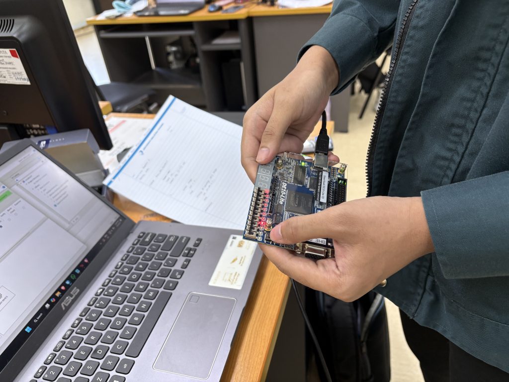
This semester in BHE3233 – Digital System Design, we’re exploring practical world of digital hardware by implementing real-time, embedded digital systems using the DE10-Lite FPGA board. Building on the fundamentals of Verilog, FSMs, and RTL design we’ve covered, students now have the opportunity to apply their knowledge through these exciting hands-on projects. Each project emphasizes different aspects of digital design—from FSM sequencing to pipelining and datapath architecture.
These projects were carefully curated to cover a wide range of course outcomes, from combinational and sequential logic design to system-level implementation using FSMs and RTL pipelines. Students not only reinforce theoretical understanding but also gain confidence in developing real-time FPGA applications using Verilog on the DE10-Lite board.
Before jumping into their projects, the students have already completed structured labs covering:-
FSM design and simulation
RTL pipelining
Clocking and timing constraints
Static timing analysis
7-segment display interfacing
Debouncing and switch inputs
These foundational skills are directly applicable to the project implementations.
Here’s a detailed look at the 6 project titles offered this semester:-
1. Morse Code Encoder and LED Blinker
Objective – Design a finite state machine (FSM)-based system that converts input characters (A-Z, 0-9) into Morse code and blinks an LED accordingly.
Key Features –
Input a hardcoded message (or via DIP switches)
FSM handles character-to-Morse conversion (dot and dash)
LED blinks in Morse timing format
Optional – Display current character on a 7-segment display during encoding
Learning Outcomes – FSM design, output timing control, sequential logic, user interaction.
2. Basic 8-bit RISC CPU Implementation
Objective – Build a basic 8-bit CPU that supports core instructions such as ADD, SUB, LOAD, STORE, and JMP.
Key Features –
4 to 8 general-purpose registers
Instruction decoder and ALU unit
ROM-based instruction memory and RAM-based data storage
Output status or values via LEDs or 7-segment display
Learning Outcomes – Datapath design, FSM for control unit, memory interfacing, and simple instruction architecture.
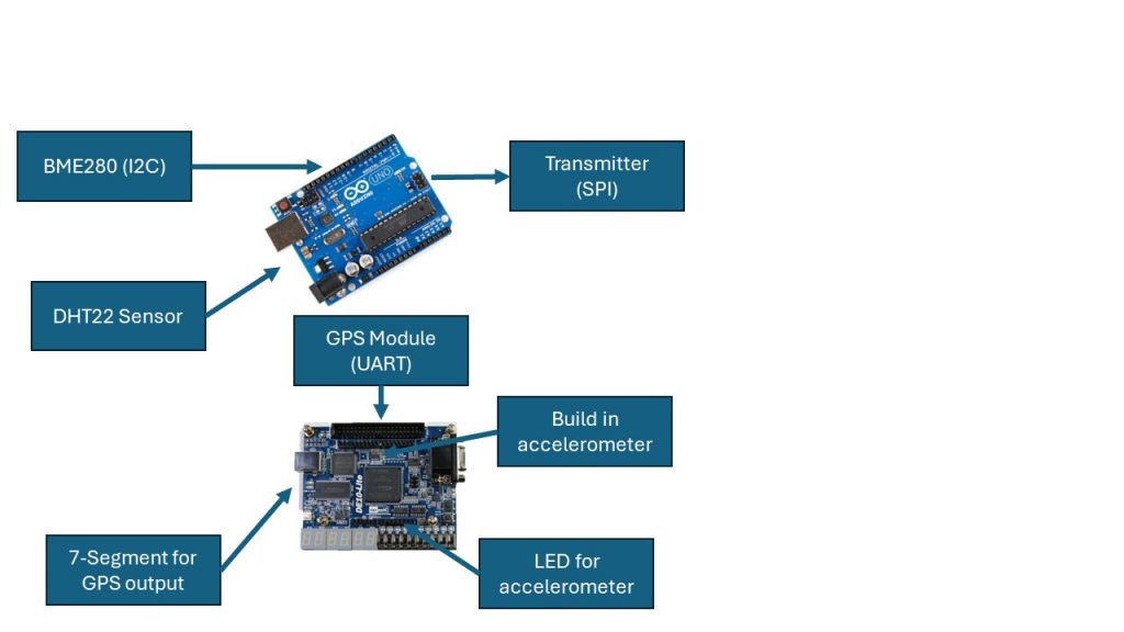
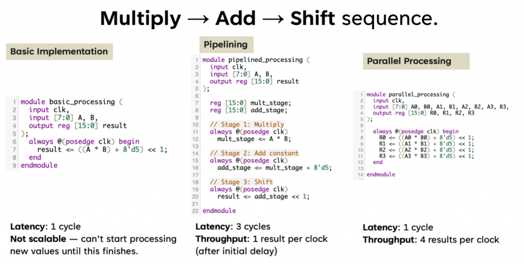
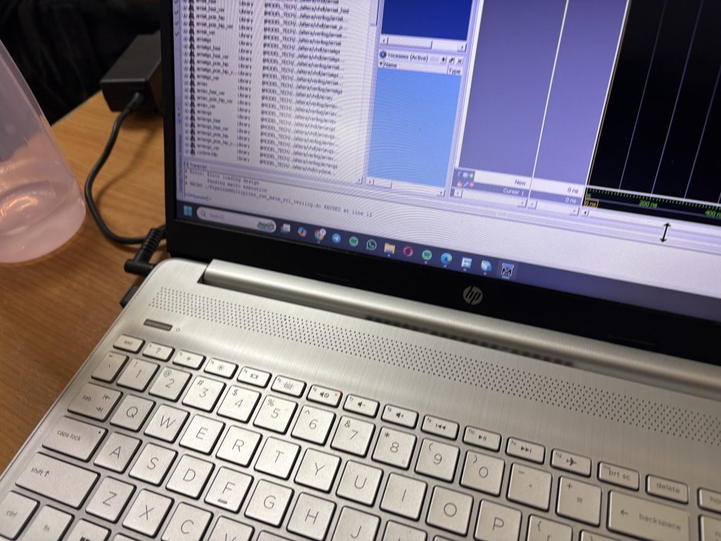
3. Parallel Multiplier Using RTL Pipelining
Objective – Design a high-speed 8-bit parallel multiplier using RTL pipelining techniques.
Key Features –
Inputs via DIP switches or pushbuttons
Multi-stage pipelining of partial products
Output result on 7-segment displays
Compare pipelined design with pure combinational multiplier in terms of:-
Critical path delay
Maximum clock frequency
FPGA logic utilization
Throughput
Learning Outcomes – Pipelined architecture, latency vs. throughput, performance analysis.
4. Digital Stopwatch with Lap Function
Objective – Create a stopwatch with basic timing functions and lap time capture.
Key Features:
Start/Stop/Reset controls via pushbuttons
FSM-based timing logic
4-digit multiplexed 7-segment display
Capture and display lap time on button press
Learning Outcomes – Sequential system design, timing counters, 7-segment multiplexing, user interface design.
Objective – Develop a digital locking system with password protection using FSM.
Key Features –
User password entry via DIP switches
Status feedback through LEDs or 7-segment
Lock/unlock logic with real-time comparison
Optional: Add retry limit and lockout on failed attempts
Learning Outcomes – FSM logic, comparison algorithms using shift registers, and embedded security logic.
6. Dice Game Controller
Objective – Simulate a simple 2-player dice game with visual feedback and turn-based logic.
Key Features –
Pushbutton to initiate dice roll
Use LFSR (Linear Feedback Shift Register) to generate pseudo-random numbers (1–6)
Output displayed using 7-segment or LED
FSM handles player turns and win conditions
Learning Outcomes – Random number generation using LFSR, FSM game logic, 7-segment display control.
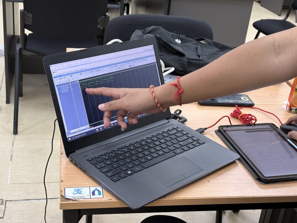
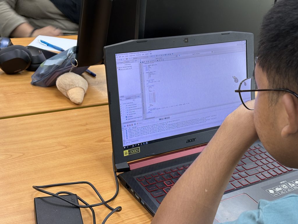
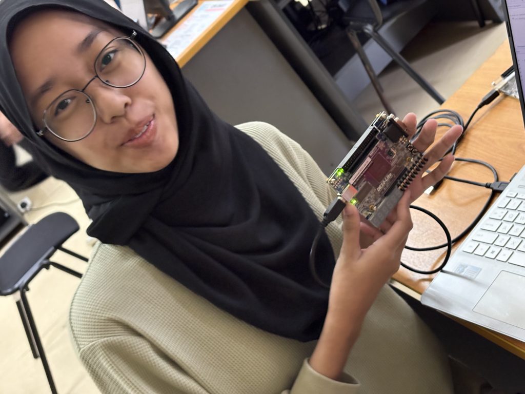
Today, each group presented their project progress. Well done!
Functional demo on the DE10-Lite board
Timing and performance analysis
Challenges and solutions in design
Looking forward to final outcome and submission in Kalam!


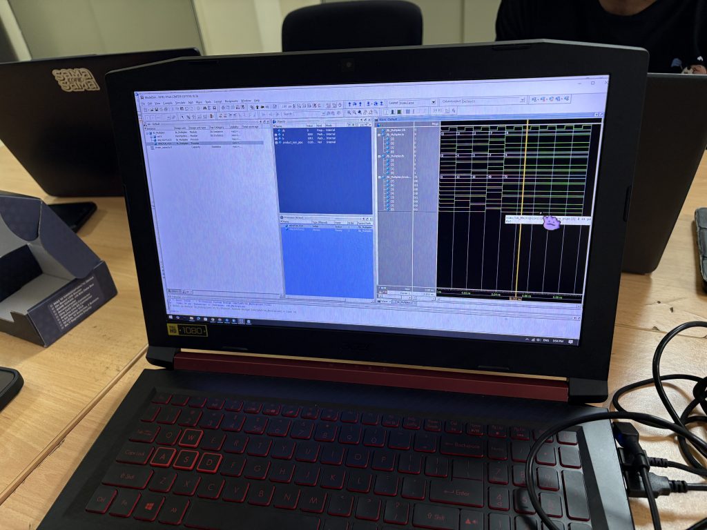
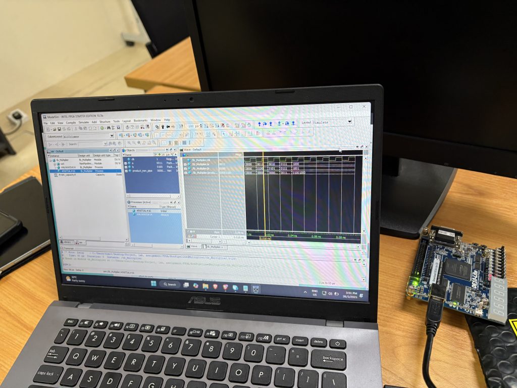
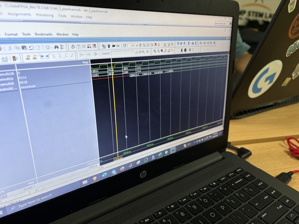
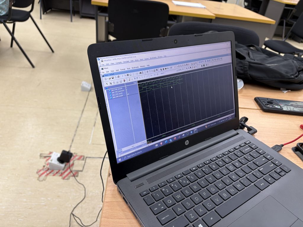
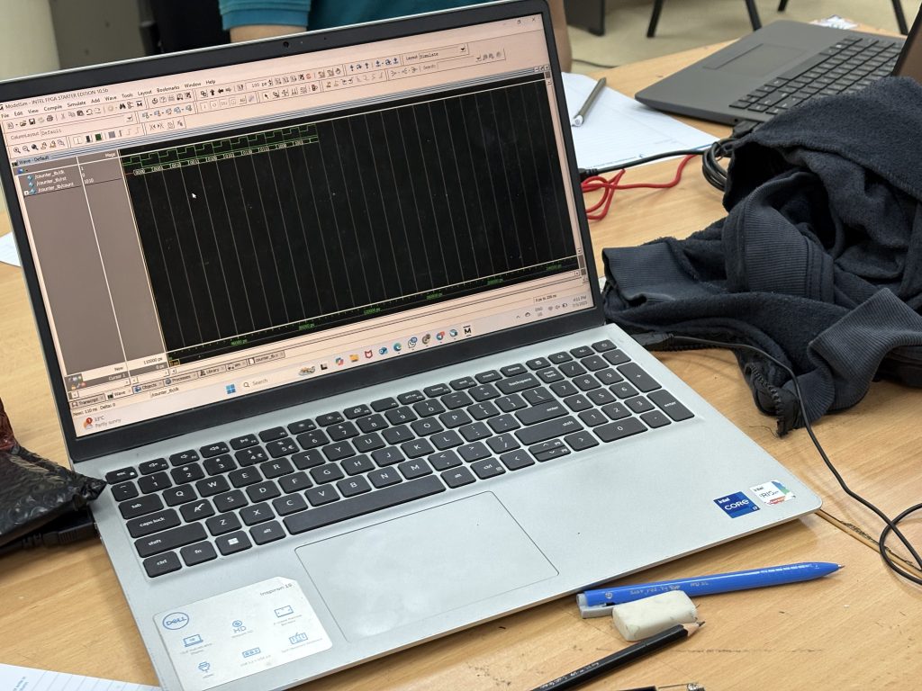
Today we look into one of the most critical yet often overlooked topics in FPGA design – Static Timing Analysis (STA). Understanding STA is key to ensuring that your digital design works not only functionally but also reliably at speed. To ground this theoretical topic, students also completed Lab 5, where they compared pipelined and non-pipelined multipliers and analyzed timing and performance parameters.
What Is Static Timing Analysis?
Static Timing Analysis is a method used to determine if a digital circuit will operate correctly at the target clock frequency without needing simulation input vectors. It uses timing constraints and logic paths to compute:
Setup time
Hold time
Propagation delay
Rise and fall times
Clock skew
Critical path delay
Maximum clock frequency
The goal is to verify that all data signals arrive where they need to, on time, under worst-case conditions.
Key Timing Parameters Explained
To help visualize the concept, we used a simple design involving two D Flip-Flops (FF1 and FF2) connected through a combinational logic block composed of two logic gates.
1. Setup Time
This is the minimum time the data must be stable before the clock edge arrives at FF2. If violated, data may not be correctly latched.
2. Hold Time
The data must remain stable after the clock edge. If violated, metastability may occur.
3. Propagation Delay
This is the time taken for the signal to travel through the logic gates between FF1 and FF2. It’s dependent on the type and number of gates.
4. Rising/Falling Time
The transition period from low to high or high to low in the signal waveform. Faster transitions are better for minimizing timing uncertainty.
5. Clock Skew
This occurs when the clock arrives at FF1 and FF2 at slightly different times. Clock skew can reduce the effective timing margin.
Example in Class Two Flip-Flops and Logic Path
Imagine a logic path between FF1 (source) and FF2 (destination)
Let’s assume-

Propagation delay through AND = 2ns
Propagation delay through OR = 3ns
Setup time of FF2 = 1ns
Clock skew = 0.5ns
Then, the total delay from FF1 to FF2 is –
To meet setup time, the clock period must be at least:
This gives a maximum clock frequency of:
In Lab 5, students implemented and tested two versions of a multiplier:
Non-Pipelined Multiplier – Straightforward, all computation happens in one clock cycle.
Pipelined Multiplier – Operation split into multiple stages with registers (flip-flops) in between.
They then analyzed the following performance metrics – (hypothetically =))
| Parameter | Non-Pipelined | Pipelined |
|---|---|---|
| Critical Path Delay | Higher | Lower |
| Max Clock Frequency | Lower | Higher |
| FPGA Logic Utilization | Lower | Higher |
| Throughput | Lower | Higher (1 output per cycle after latency) |
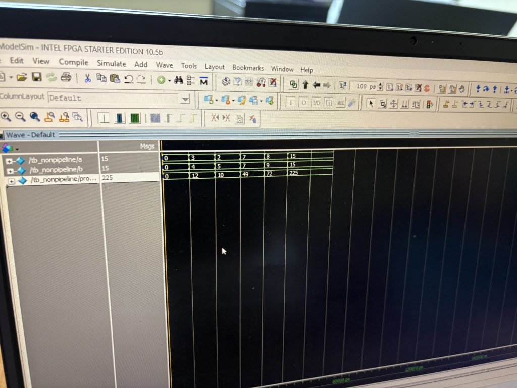
Pipelining reduces the critical path delay, allowing the design to run at a much higher clock frequency.
While pipelining increases the logic utilization (more flip-flops), the throughput improves significantly, making it ideal for high-speed applications like real-time data processing in picosatellites or image processing.
Static timing analysis helps quantify the improvements, giving insight into real performance beyond just functional correctness.
See you next week for your FPGA project development =)
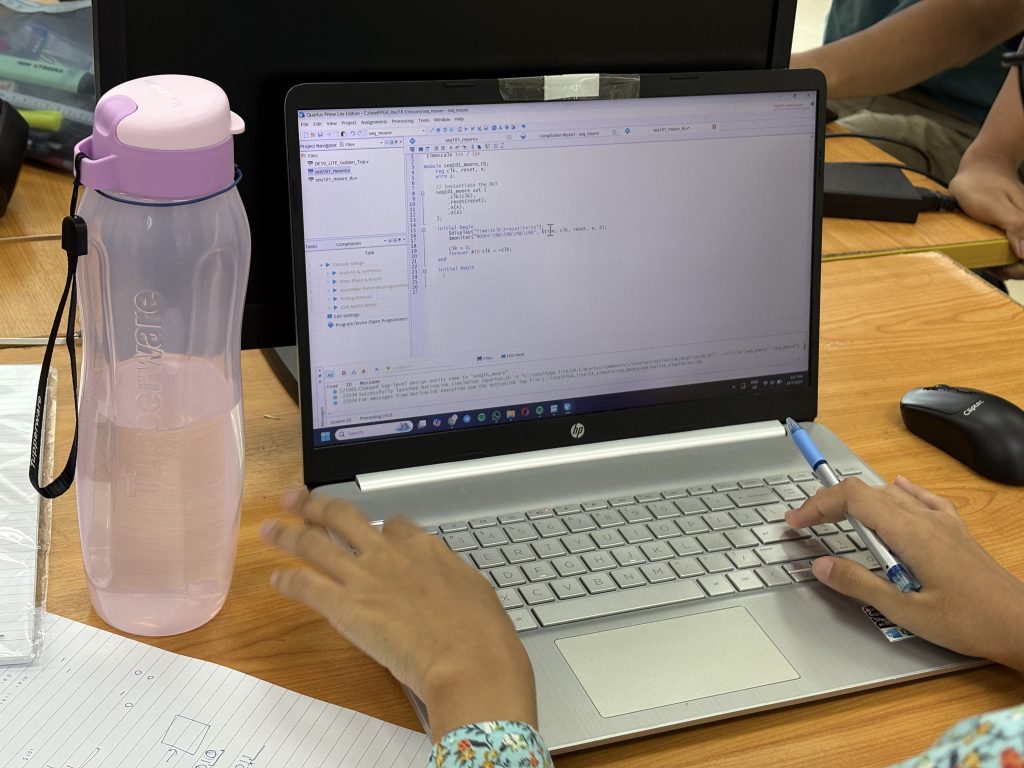
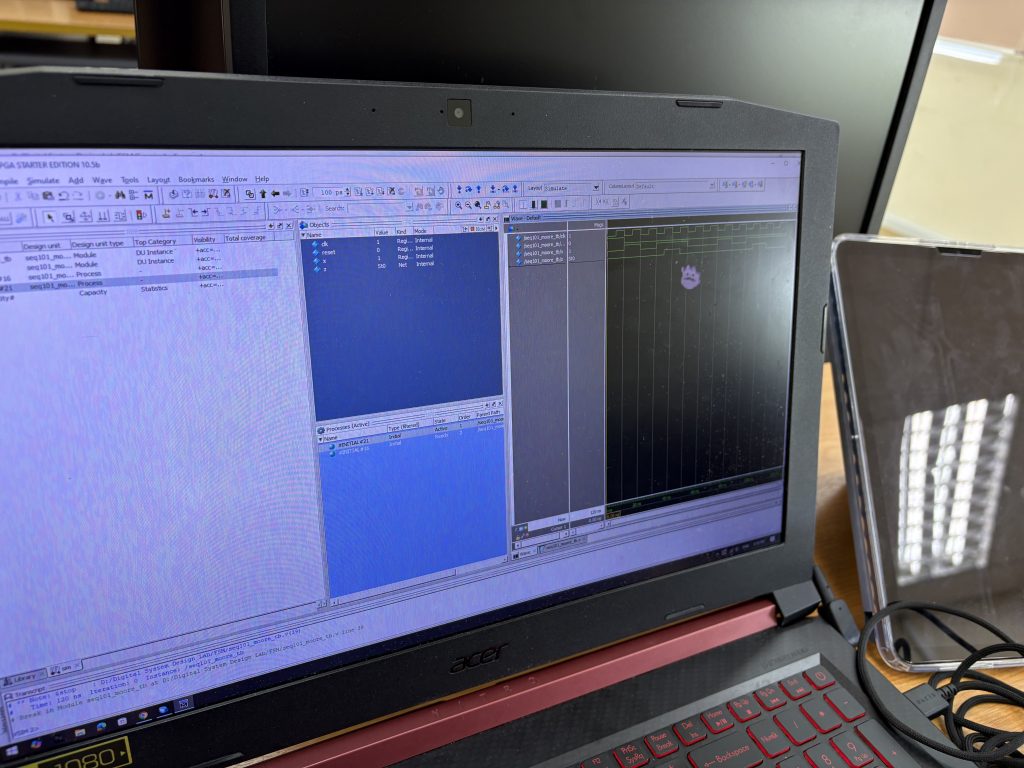
Today’s class focused on one of the core topics in digital system design—Finite State Machines (FSM)—through an engaging and practical activity: building a 101 sequence detector using a Moore machine.
We began with a recap of FSM fundamentals—specifically the Moore machine, where outputs are solely determined by the current state. This conceptual understanding paved the way for the day’s main activity: designing and testing a sequence detector that identifies the binary pattern 101.
Key areas explored:
State transition diagrams and state encoding
Implementation using case statements
Exploring both dataflow-style FSM and conditional (if-else) statement-based FSMs
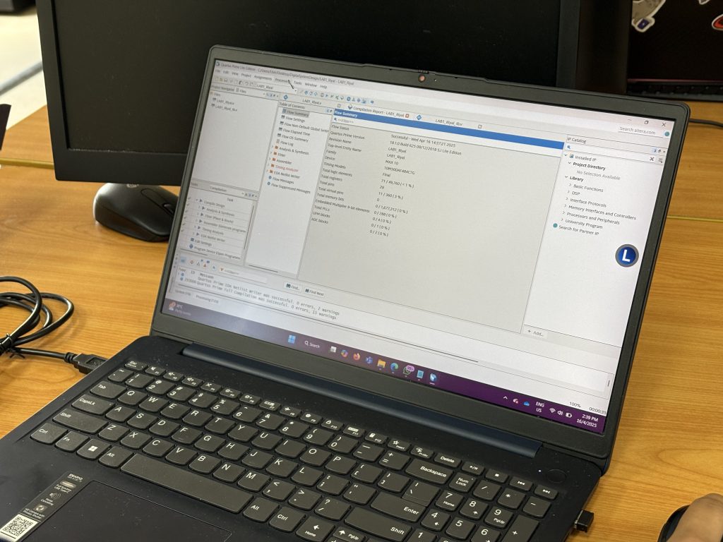
Synthesizing and testing using Quartus Prime
Students designed the FSM in Verilog using Quartus. The Moore machine was structured with three states to detect the pattern:
S0 – Initial state
S1 – Received ‘1’
S2 – Received ‘10’
When the full sequence 101 was detected, the FSM output went high.
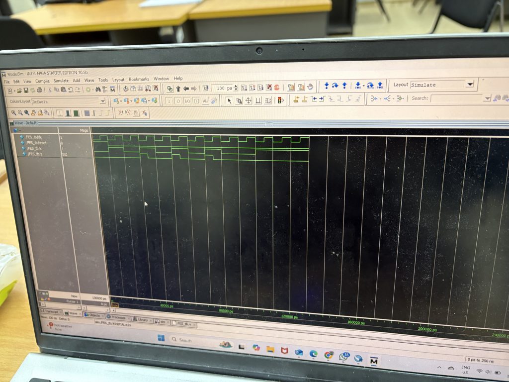
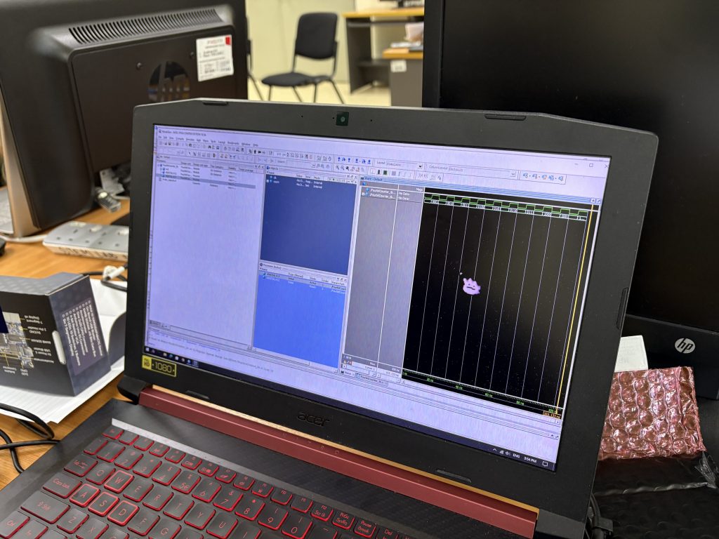
Simulation and Testbench Creation
To validate the design, students created testbenches that simulated input sequences. Using ModelSim, they:
Applied a sequence of 0s and 1s to the in input
Monitored state transitions
Verified output pulses when 101 was detected
This phase helped students understand the role of simulation in design verification and how FSMs react to clocked inputs in real time.
The case statement simplified FSM implementation, especially when compared to nested conditional (if-else) logic. They also discussed how a well-structured FSM can lead to clean, readable, and maintainable RTL code—an essential practice in real-world design.
Learning Outcomes
By the end of the session, students were able to:
Describe and implement Moore FSMs in Verilog
Translate a sequence detection problem into state transitions
Use Quartus for synthesis and ModelSim for simulation
Compare dataflow FSM vs. conditional FSM modeling

Counter and multiplexer. Well done.
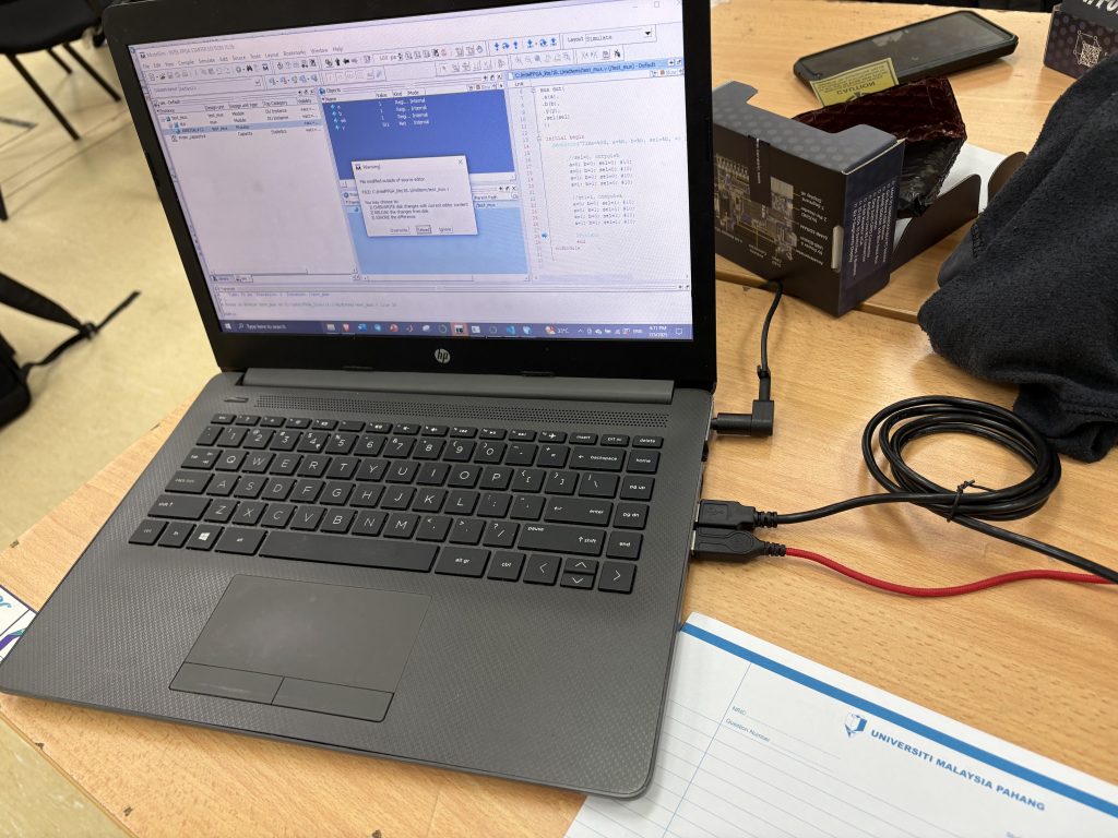
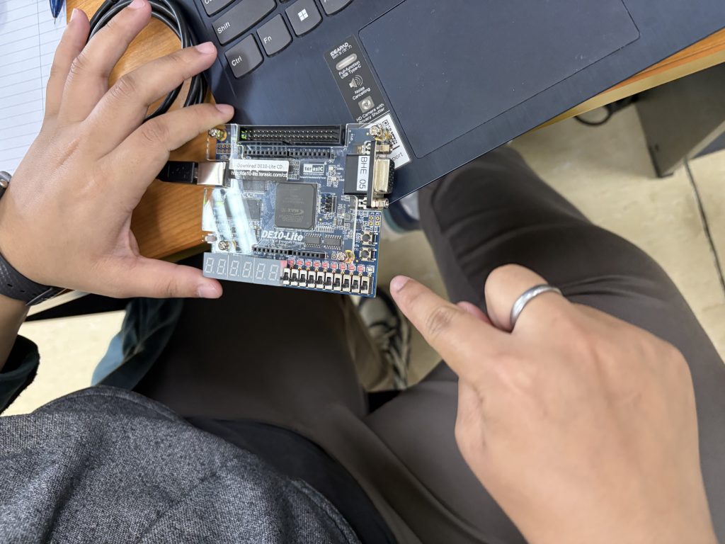
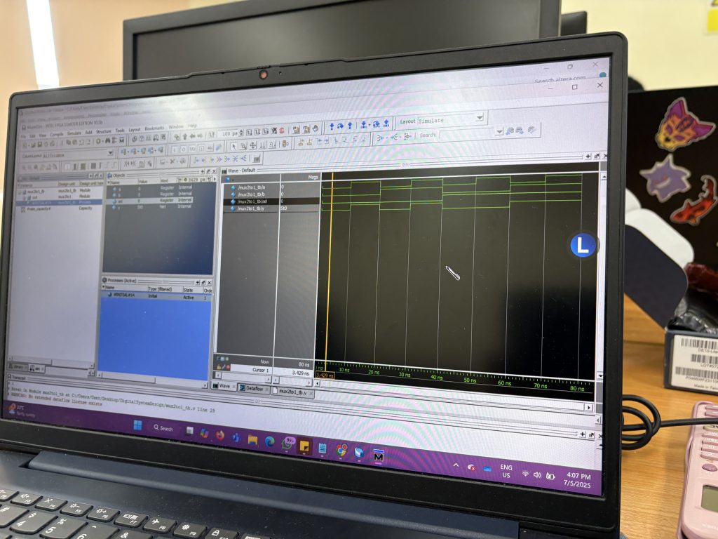
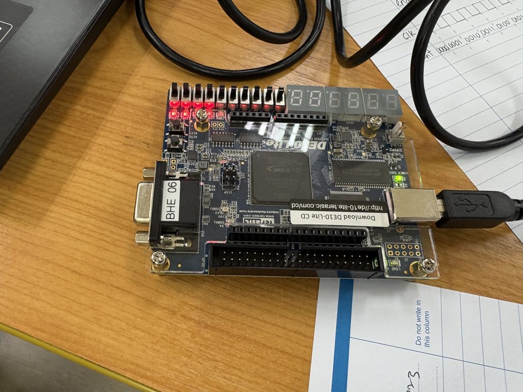

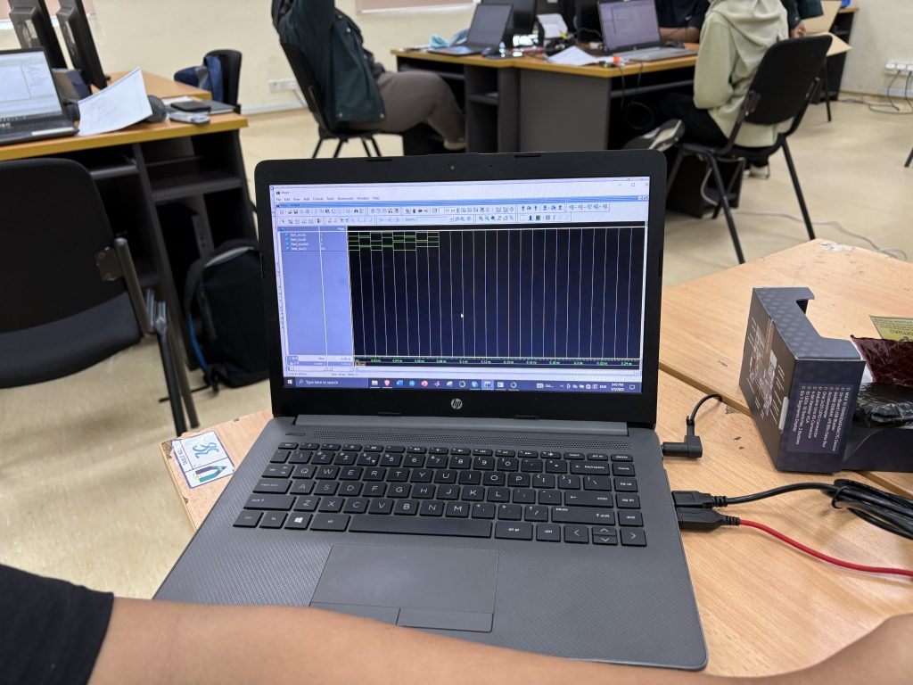
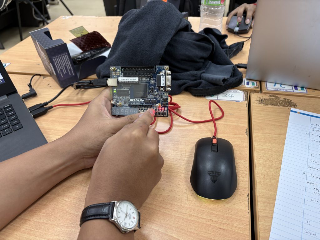
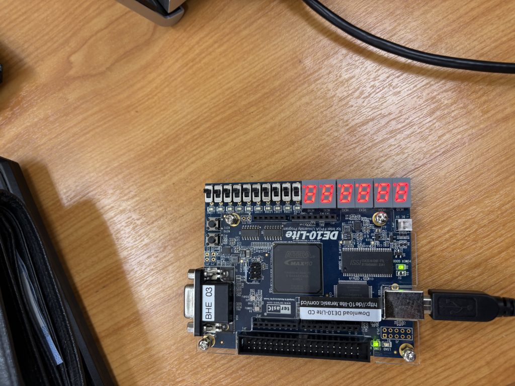
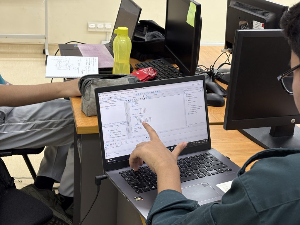
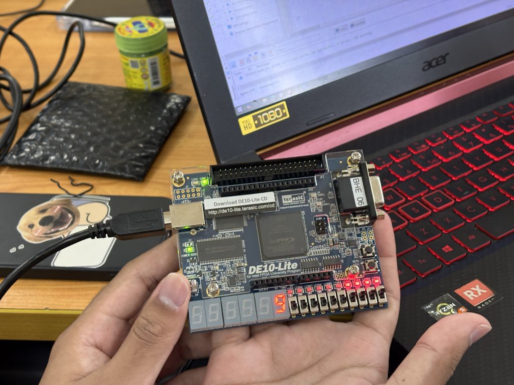
This week, students in the BHE3233: Hardware Description Language course took on three lab activities using the Altera DE10-Lite FPGA board. These labs were designed to deepen their understanding of digital logic design, from real hardware control to simulation-level debugging using testbenches.
Lab 1 Recap: LED Blinking with Verilog
Students developed a Verilog module to blink the 10 onboard LEDs one at a time in sequence, based on a timing counter. The project introduced:
always @(posedge clk)
Counter logic for delay generation
reg and assign statements for driving output
Pin assignment in Quartus
Lab 2 Recap: Real-Time LED Control Using Slider Switches
Students mapped the 10 slider switches directly to the 10 LEDs using basic combinational logic. This hands-on activity helped reinforce:
Use of continuous assignment (assign)
Bit-wise mapping between inputs and outputs
How to apply pin mapping in Quartus for SW[9:0] and LED[9:0]
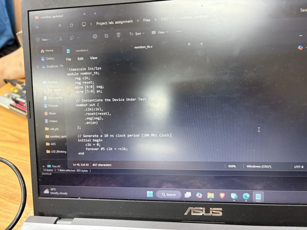
Lab 3 Preview: Writing a Testbench & Understanding Timing Diagrams
To develop a testbench for both Lab 1 (LED Blinking) and Lab 2 (Switch to LED) designs, simulate the behavior using ModelSim, and interpret the timing diagram (waveform) to verify correct functionality.
ModelSim (Intel FPGA Edition) for running simulations
Waveform viewer for analyzing signal transitions over time
To Do
Create a Testbench File for Each Design
Instantiate the DUT (Design Under Test)
Simulate clk signal (for Lab 1)
Apply appropriate test vectors (SW[9:0]) for Lab 2
Run Simulation
Launch ModelSim from Quartus
Compile and simulate the testbench
Observe and save waveform output
Analyze the Timing Diagram
For Lab 1: Check the blinking behavior of LED[current_led]
For Lab 2: Confirm that LED outputs match the SW inputs at each simulation step
Learning Outcome:
Students will visually interpret digital signal transitions through the waveform viewer in ModelSim, reinforcing:
Propagation delay
Clock edge behavior
Signal assertion and response timing

Apply Hardware Description Languages (HDL) to design, simulate, and verify digital circuits at the Register Transfer Level (RTL).
Lab 3 bridges the gap between coding and functional verification. Students now understand how simulation helps confirm logic correctness before moving to hardware.
What’s Next?
Next week, you will begin working on combinational building blocks like adders and multipliers, then explore state machines and RTL synthesis in depth.
and Midterm Test 🙂


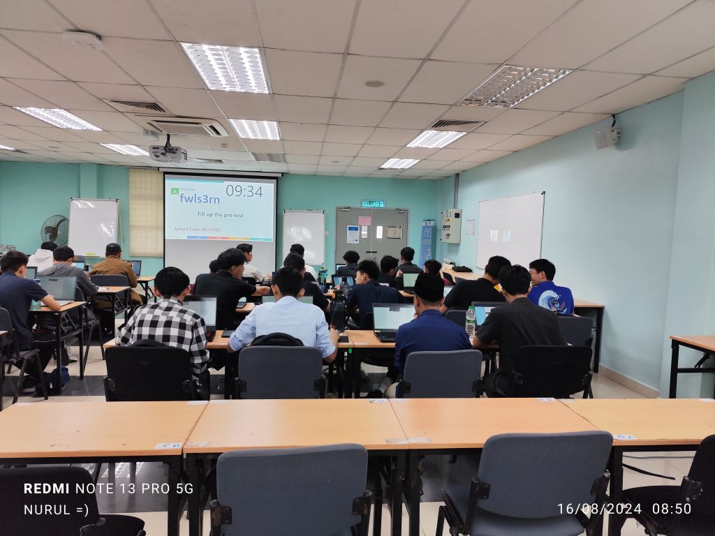
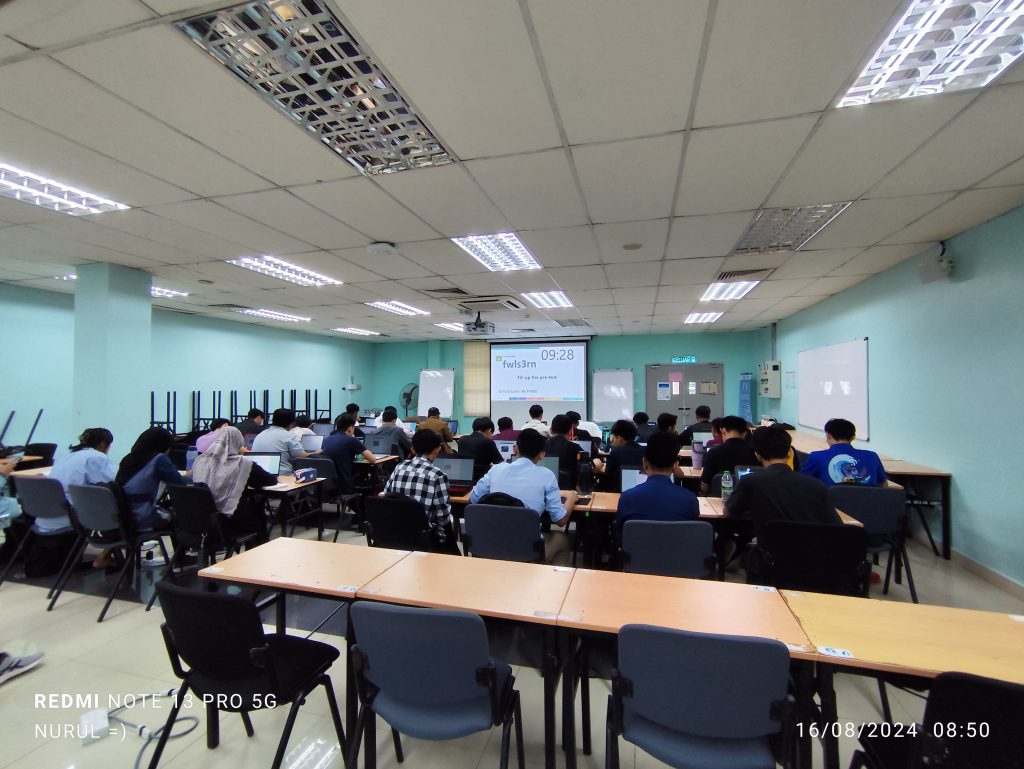
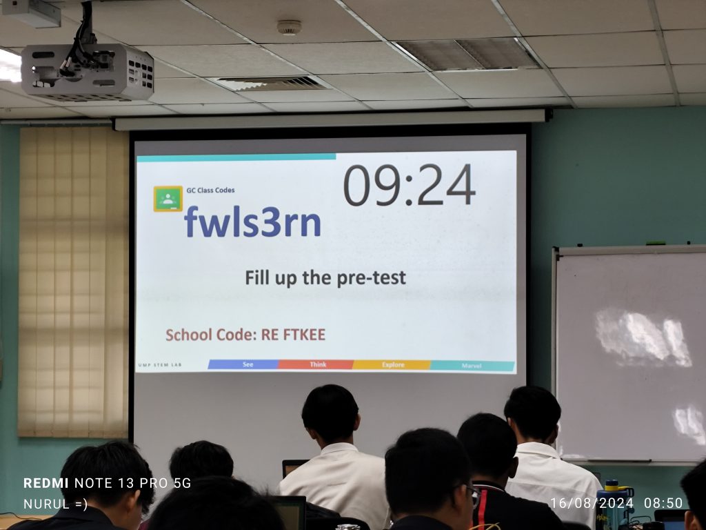
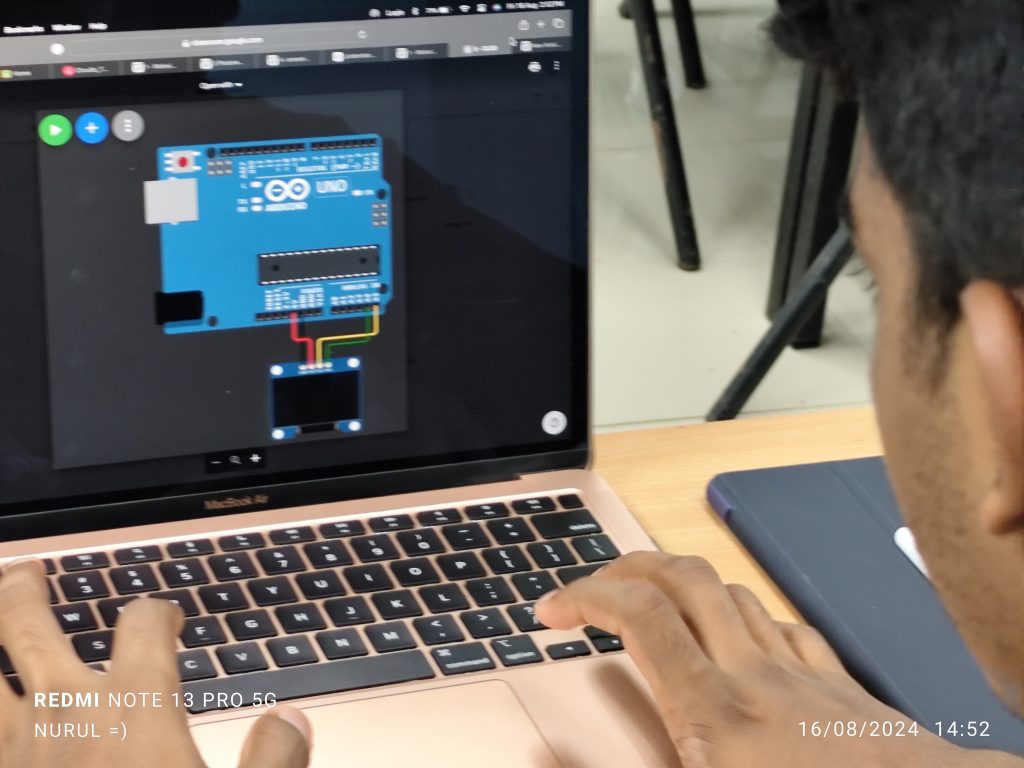
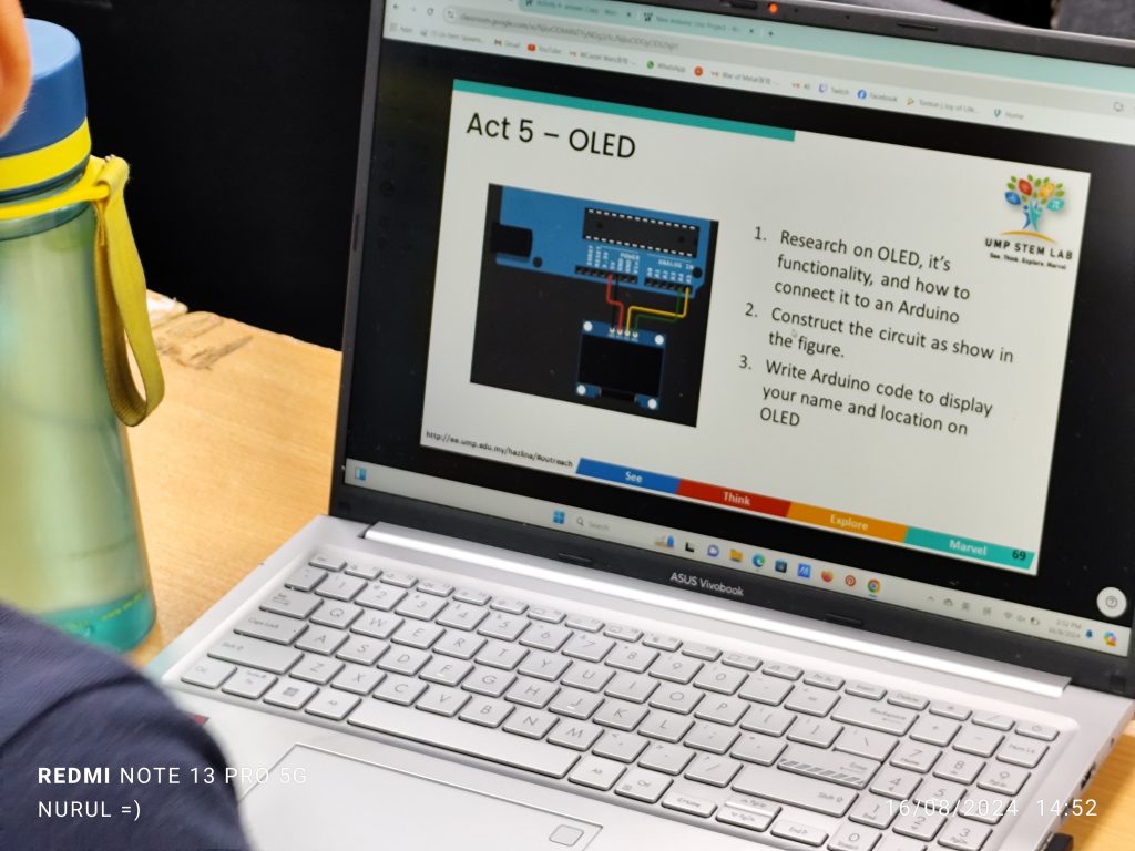
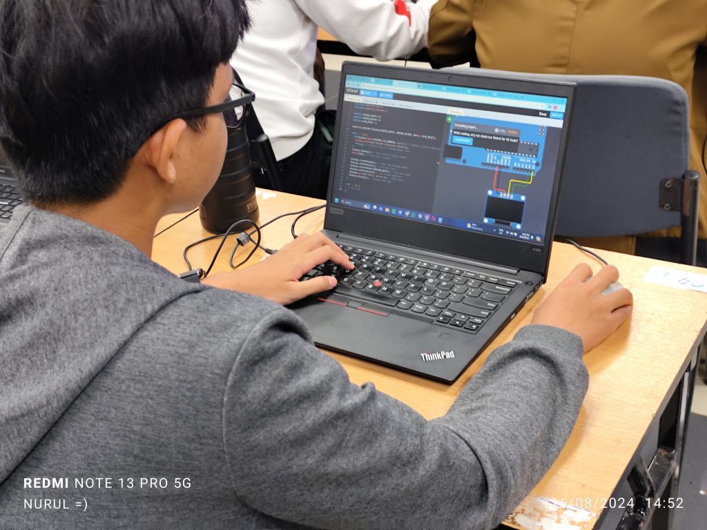
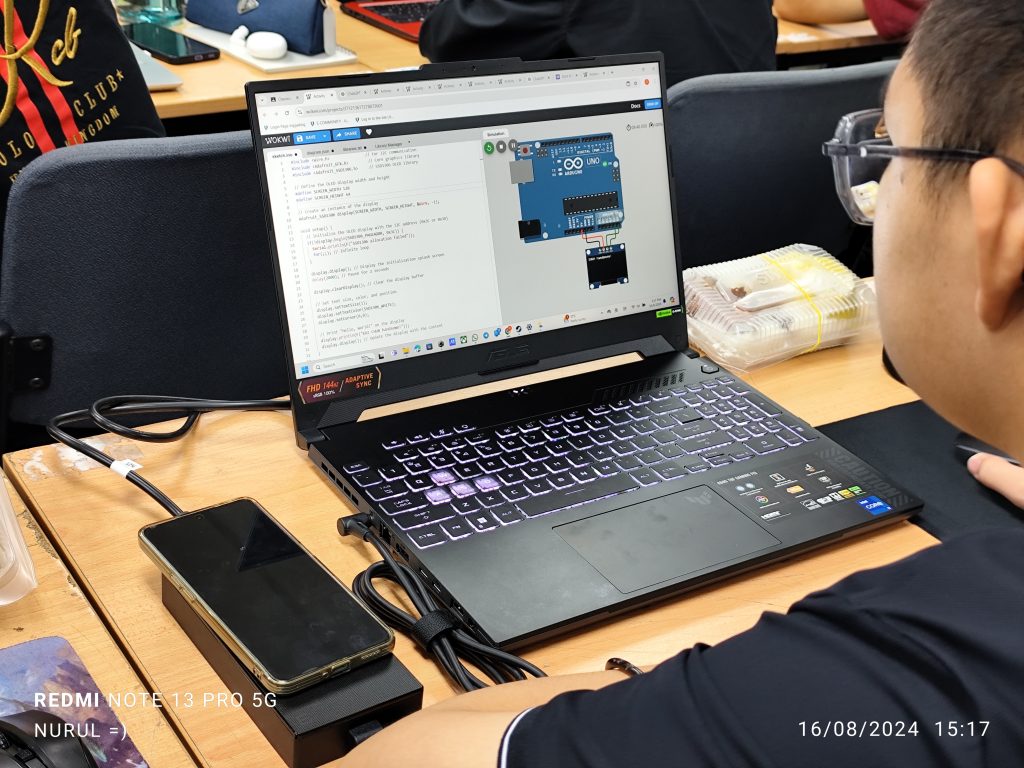
Synopsis on AI Assisted Learning @UMPSA STEM Lab module.
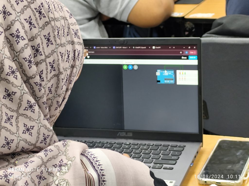
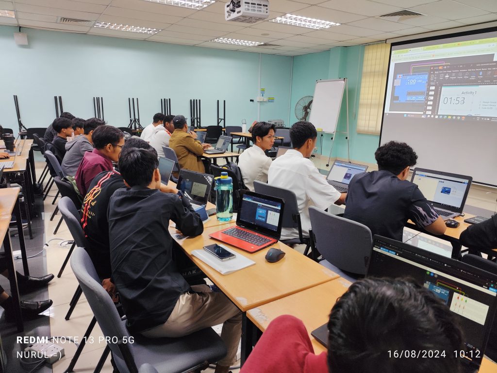
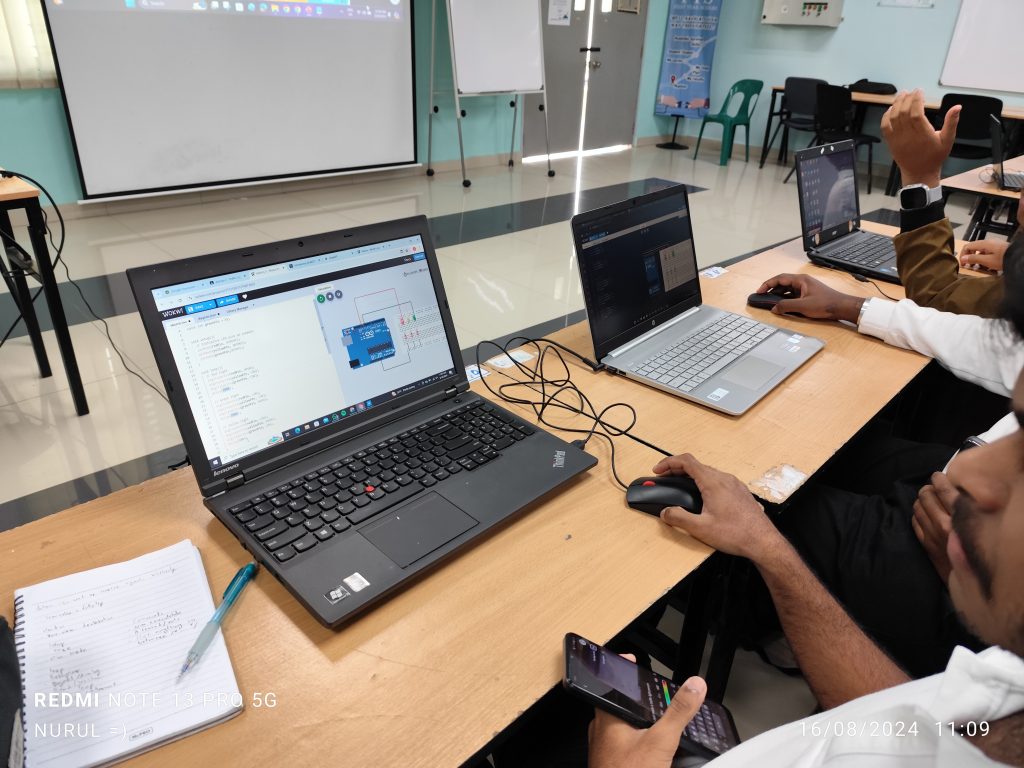
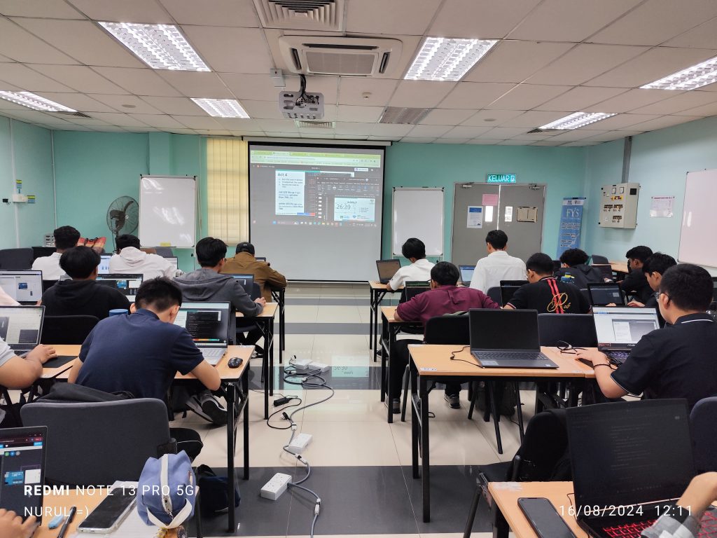
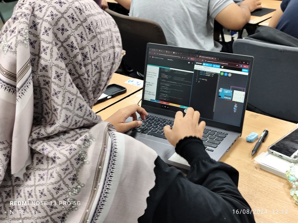
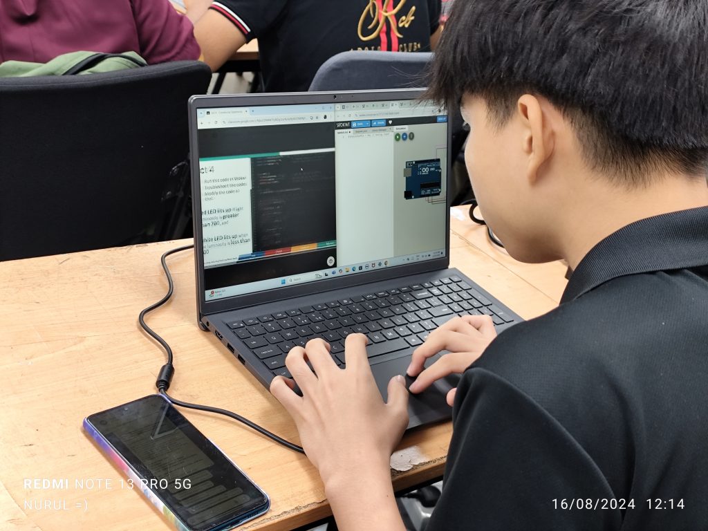
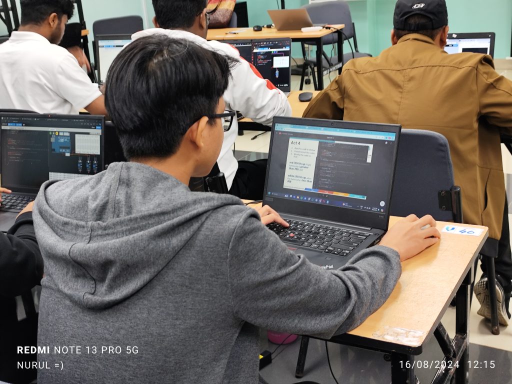
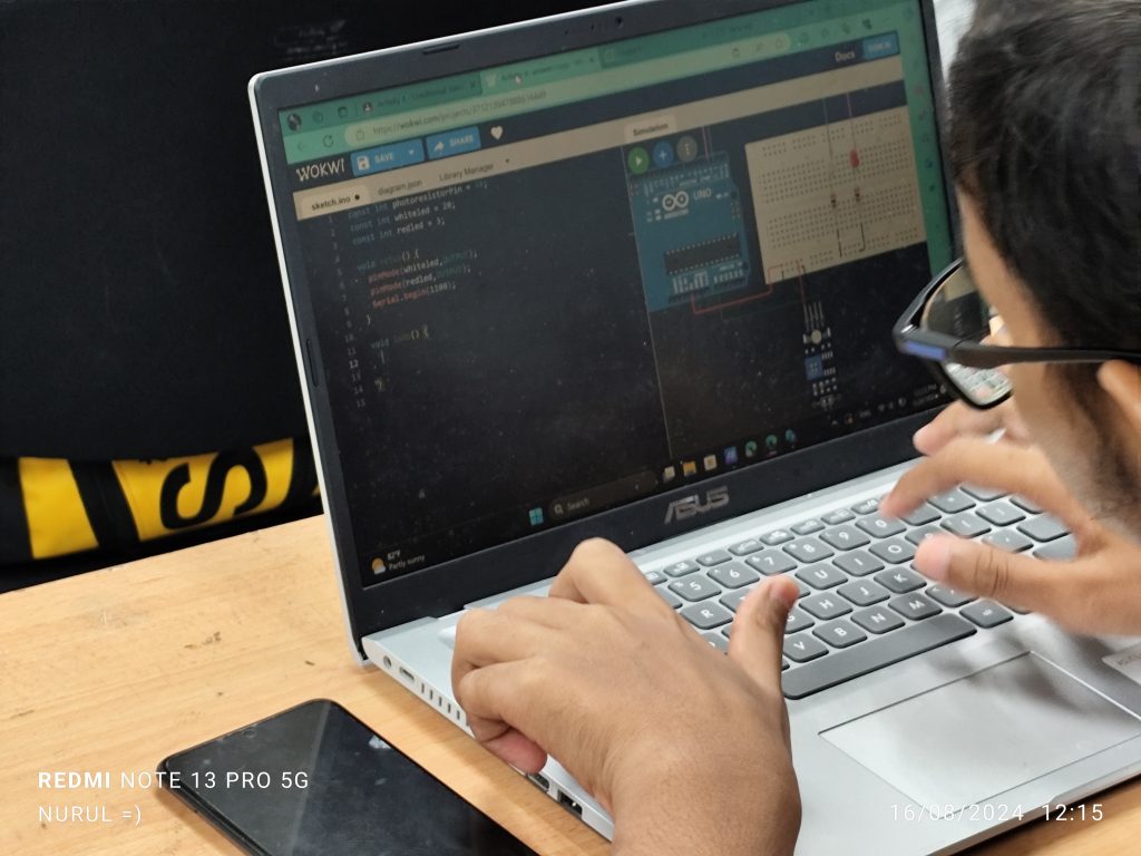
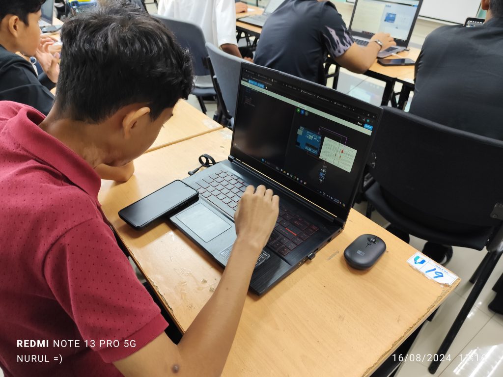
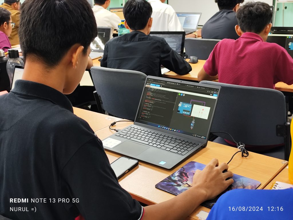
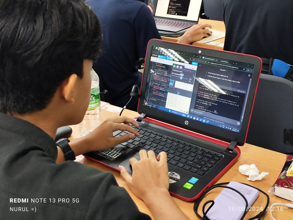
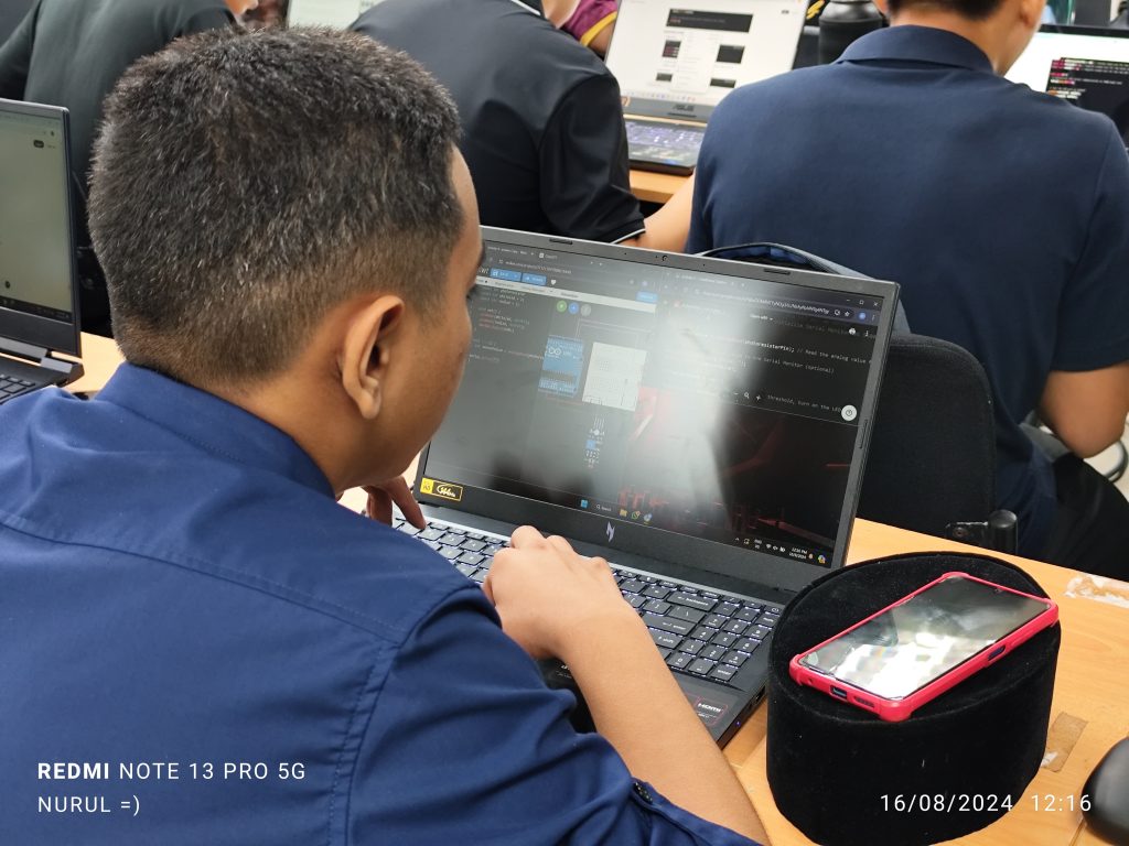
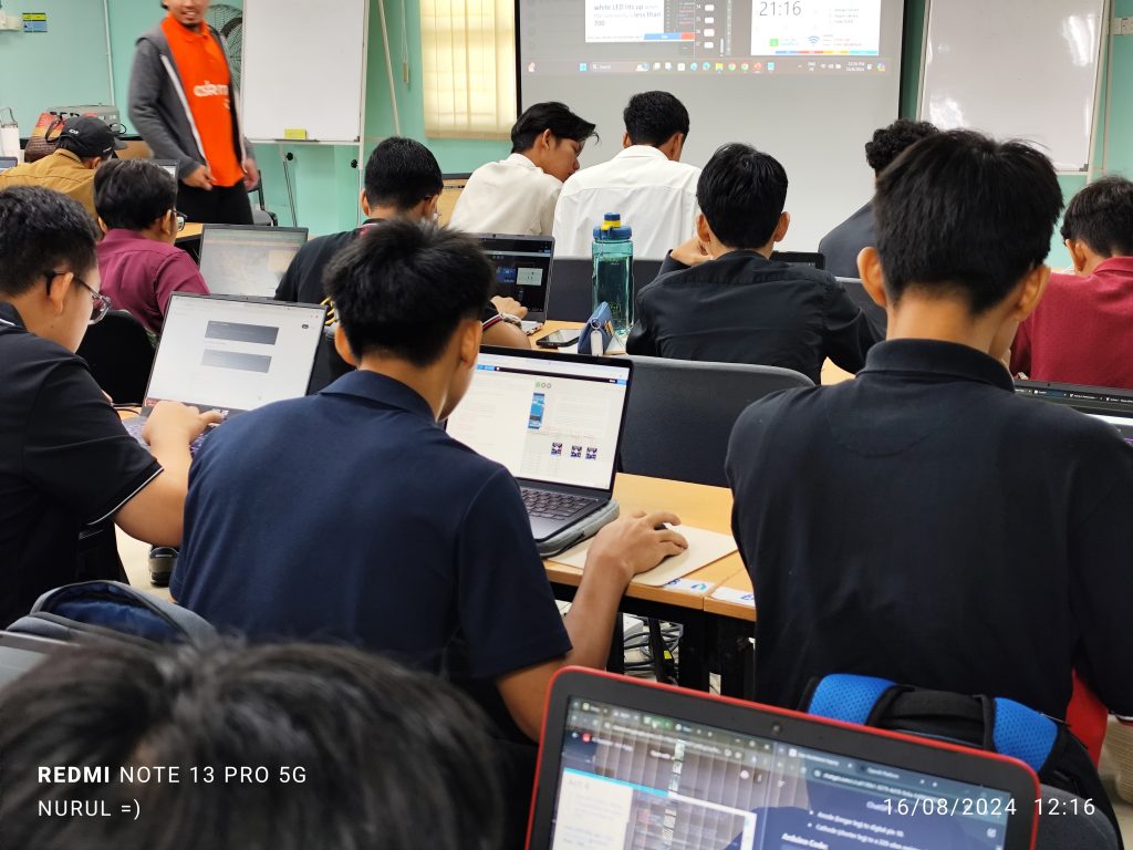
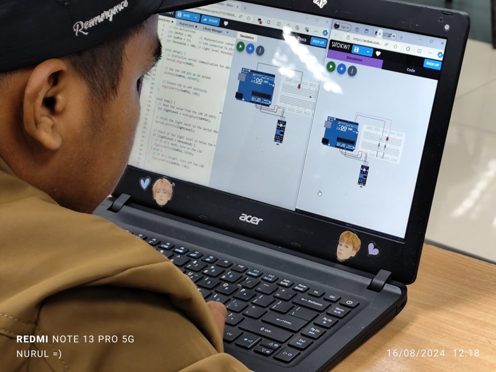
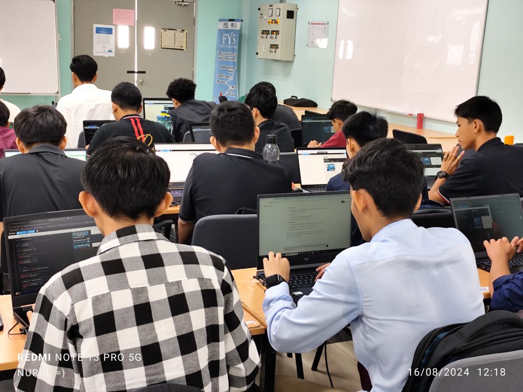
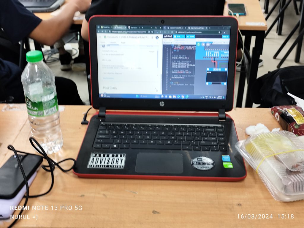
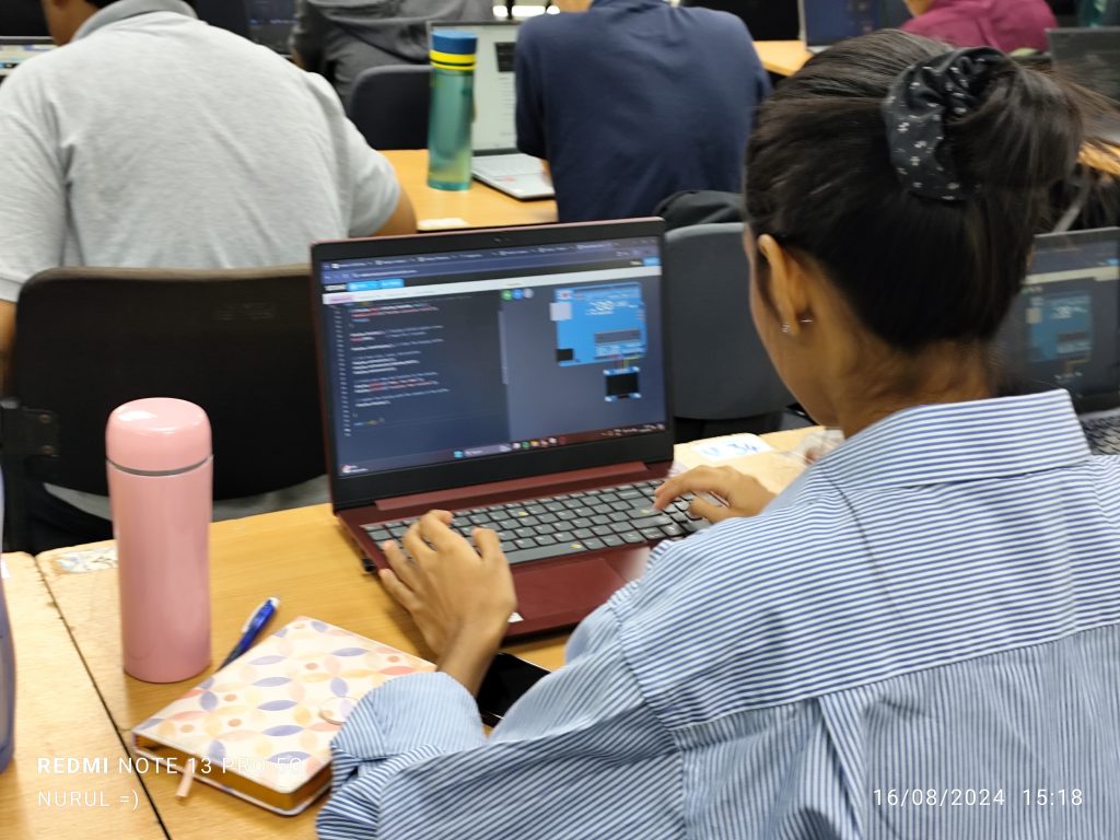
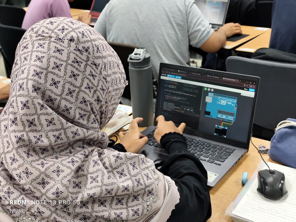
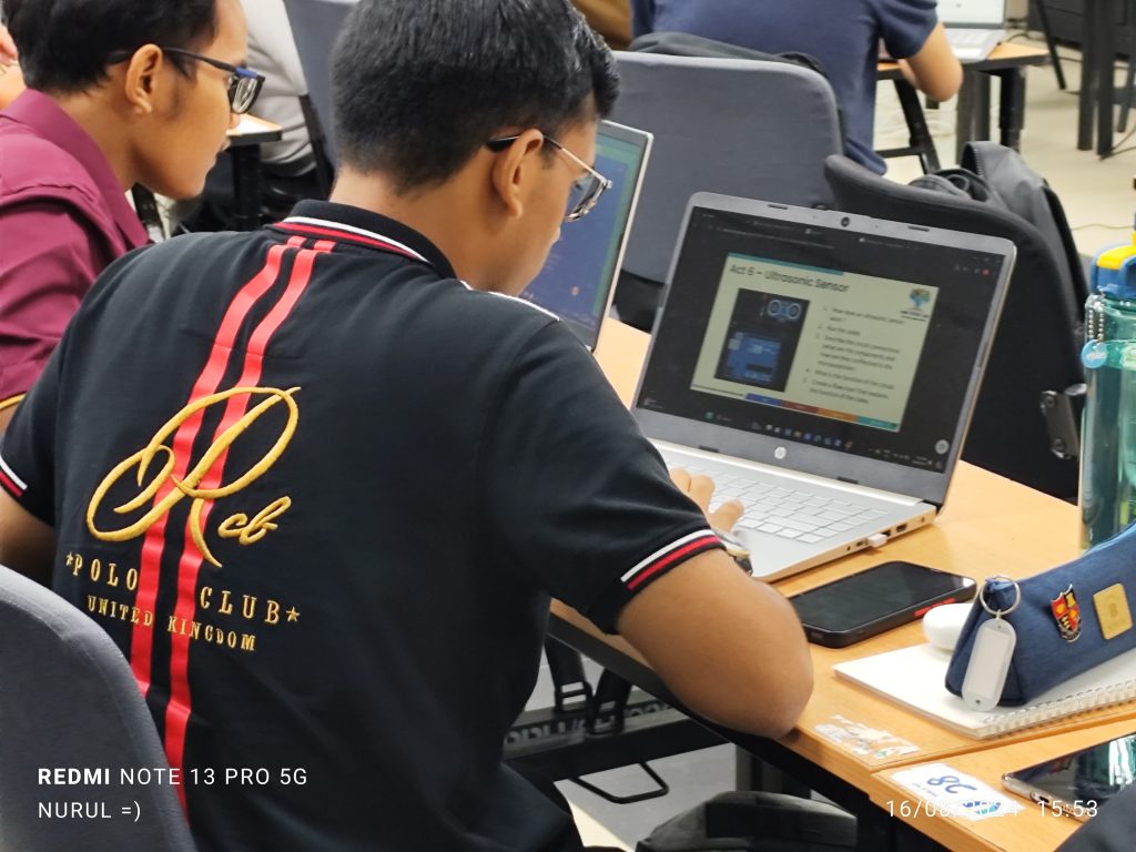
Today’s session involves interactive session for 32 first-year Electrical & Electronics Engineering students. These students, in their very first semester, were taking their initial steps into the world of computer programming and physical computing. Despite having no prior experience, they embarked on a journey that introduced them to the power and potential of AI-assisted learning.
The session was designed with a clear objective to demystify the basics of Arduino programming and physical computing while leveraging AI tools to make the learning process more intuitive and accessible. For many of these students, this was their first exposure to the intricacies of coding and the fascinating world of microcontrollers. The use of AI in the learning process provided a significant boost, enabling them to grasp complex concepts more easily and with greater confidence.
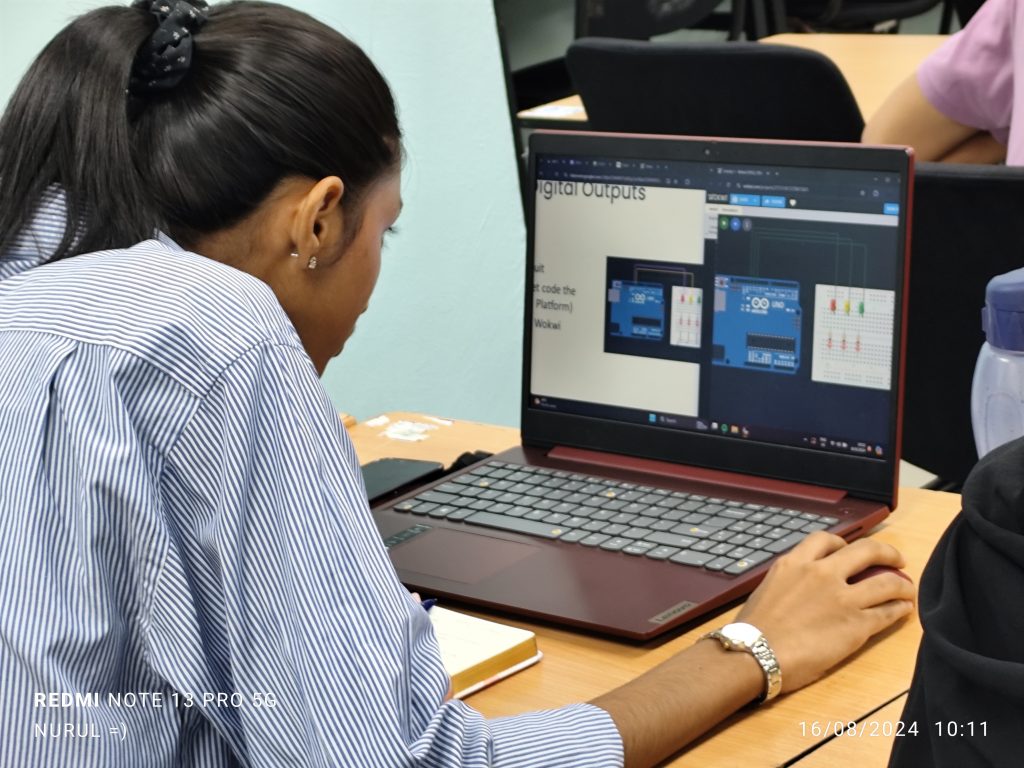
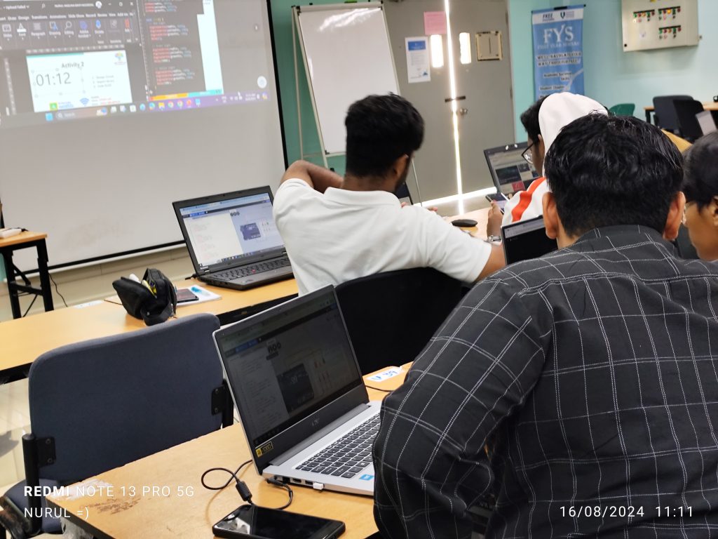
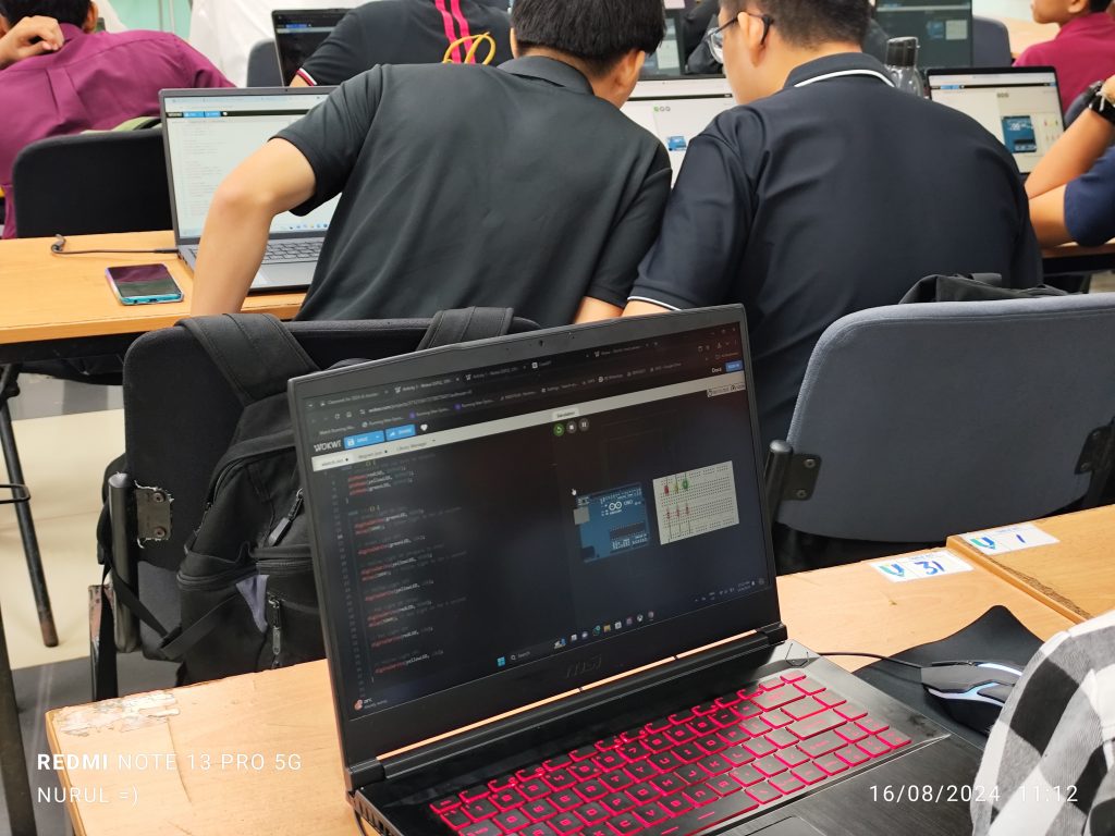
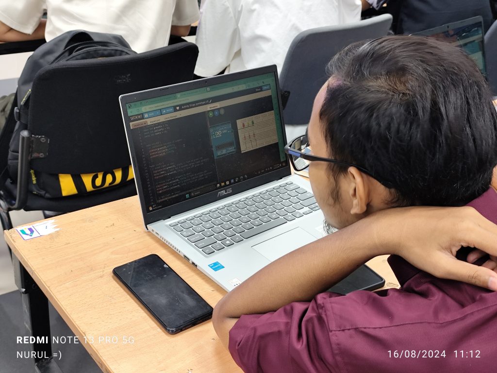
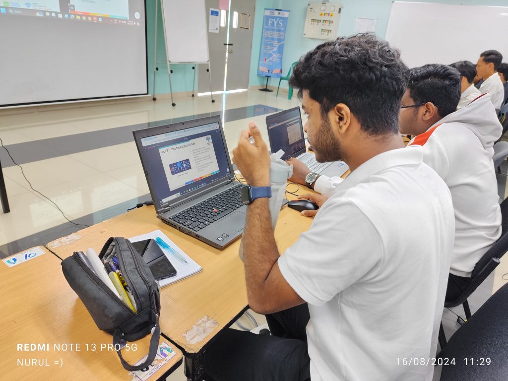
The essence of the session was a series of six hands-on activities, each carefully crafted to build upon the previous one, ensuring a gradual yet comprehensive learning experience. These activities were designed not only to teach the basics of programming and electronics but also to illustrate how AI can be a valuable ally in the learning process.
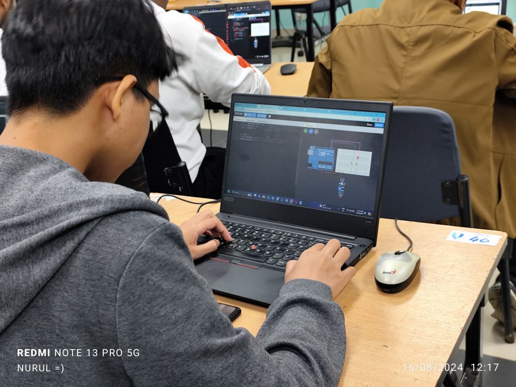
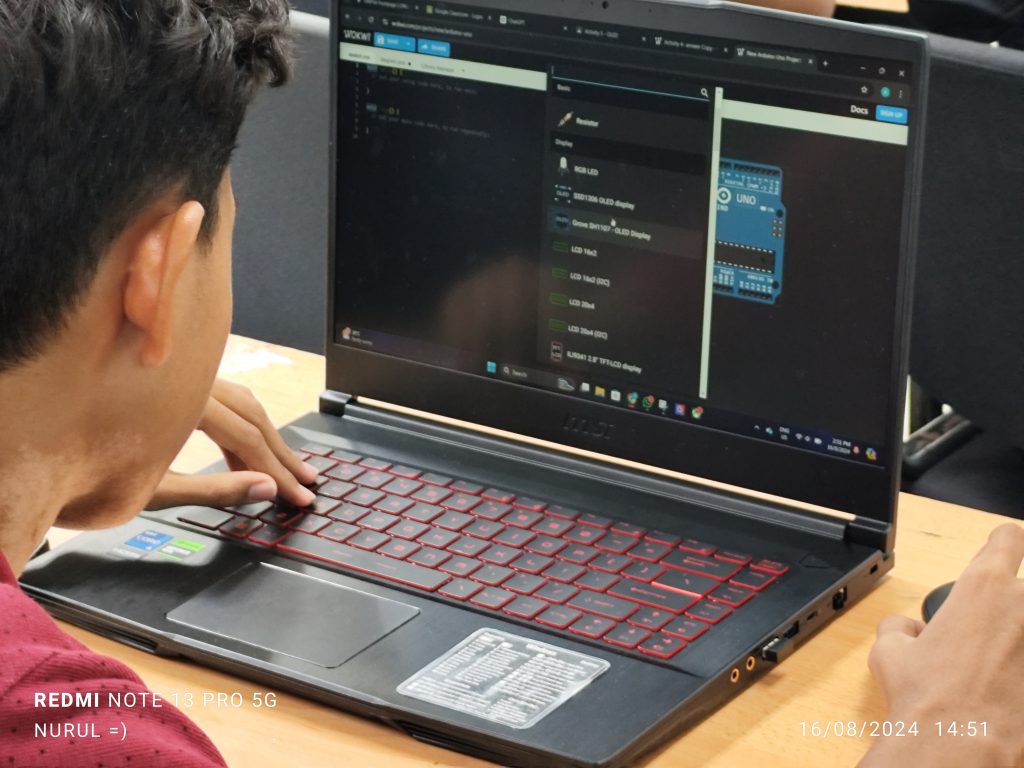
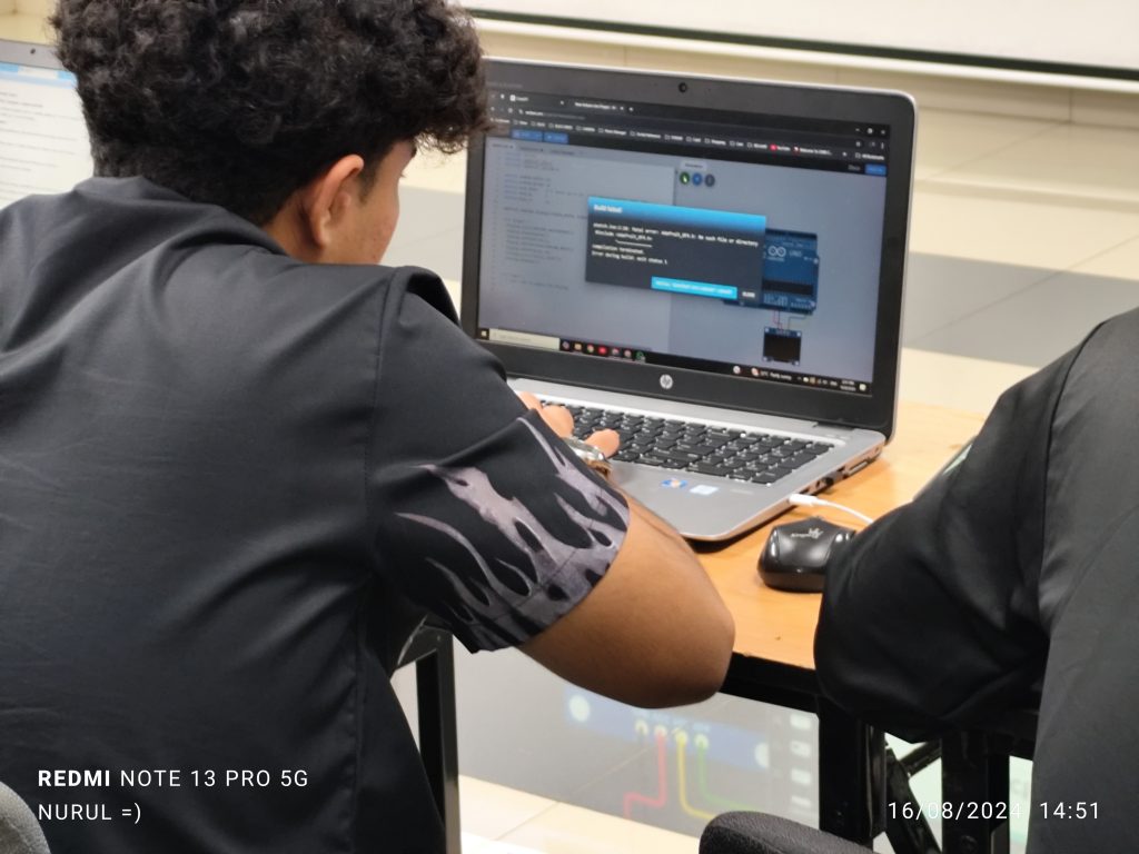
During the session, students were introduced to the Arduino platform, gaining a solid understanding of its components and the vast potential it holds for creating interactive projects. This foundational knowledge was crucial as it set the stage for the more complex tasks that followed. Leveraging AI tools like ChatGPT, students witnessed firsthand how AI could assist in generating and debugging code, making the learning process more efficient. This activity demonstrated the practical benefits of AI, especially in reducing the learning curve for beginners.
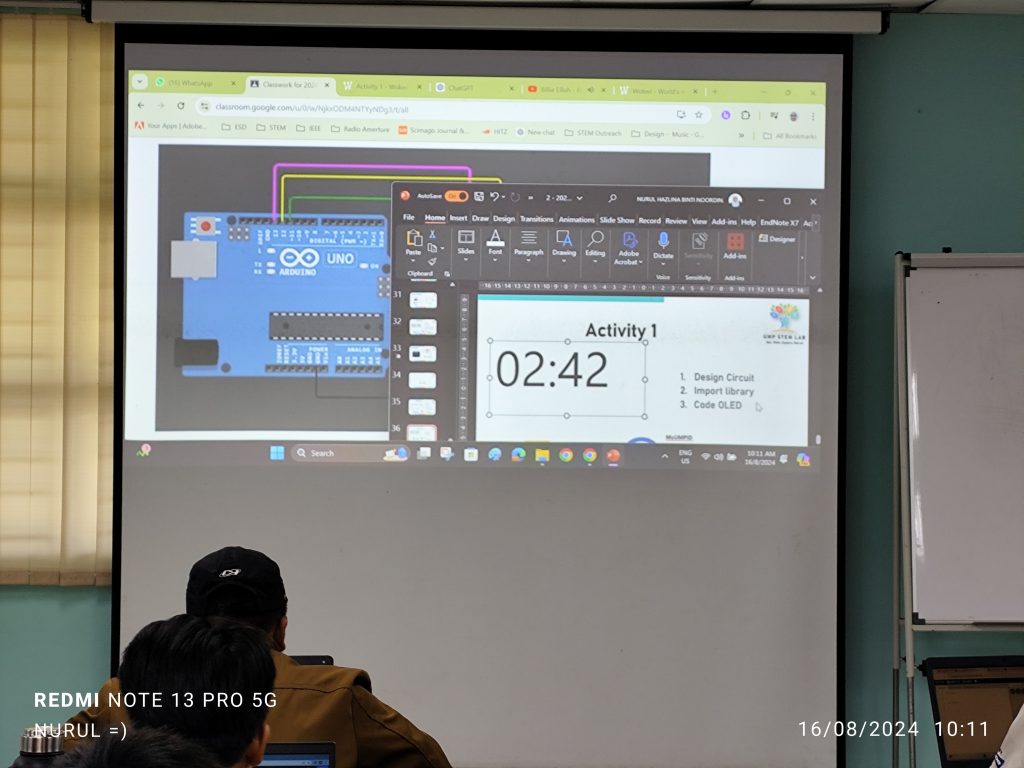
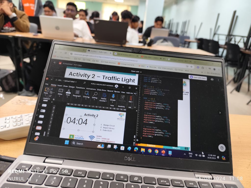
As they progressed, the students engaged in the classic “Hello World” of Arduino by writing simple code to control an LED, an experience that built their confidence and deepened their understanding of digital outputs. The next step in their learning journey was the traffic light simulation project, where they applied control structures to manage multiple outputs. This project not only taught them the intricacies of timing and logic but also encouraged them to think critically about how these elements interact in real-world applications.
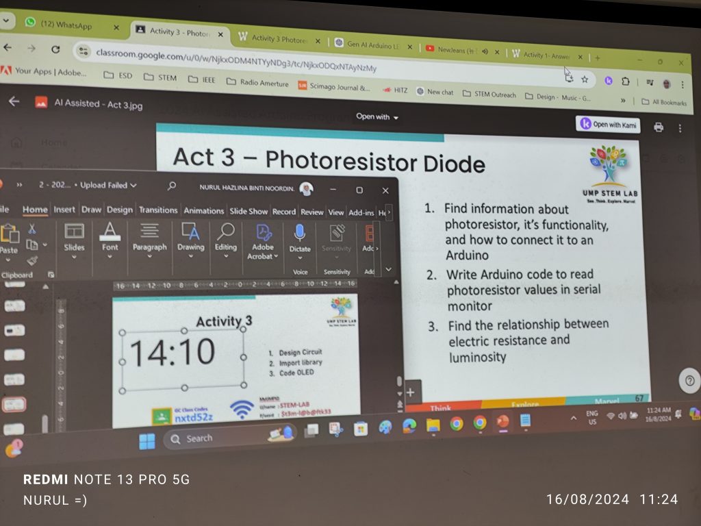
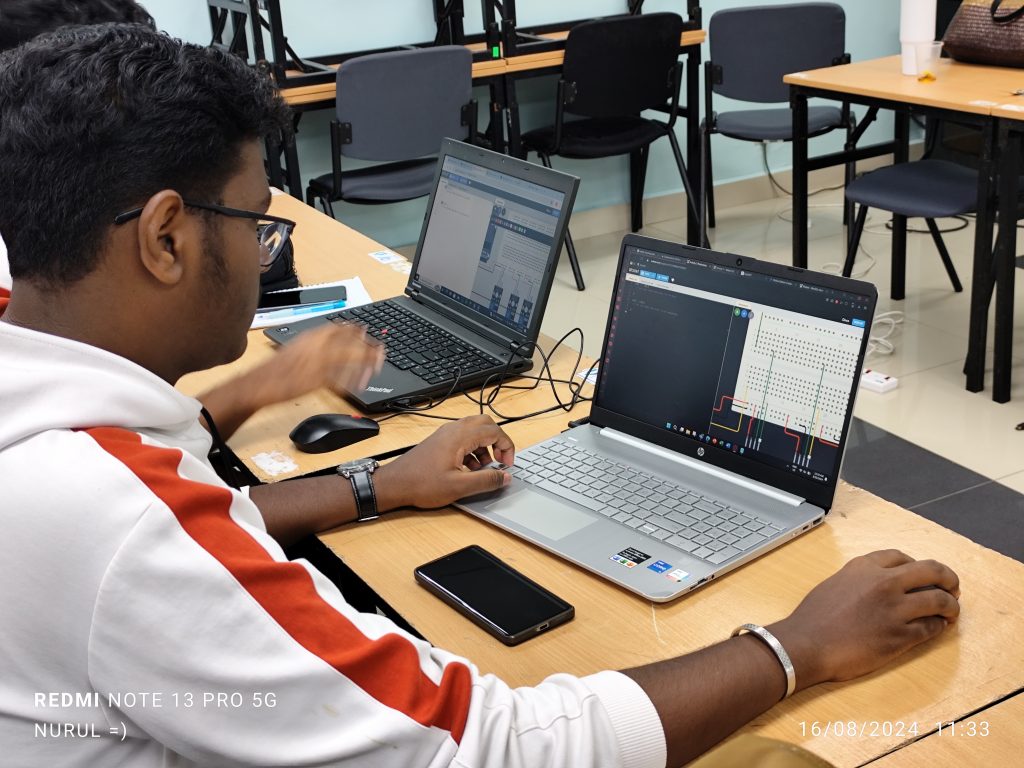
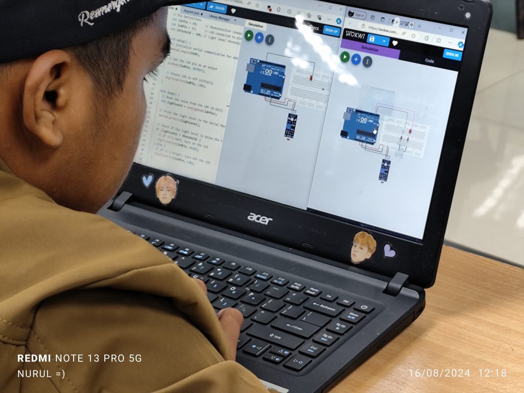
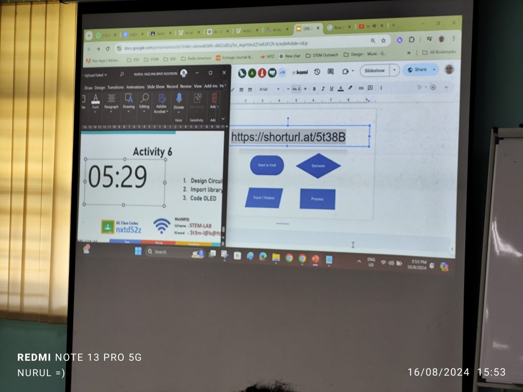
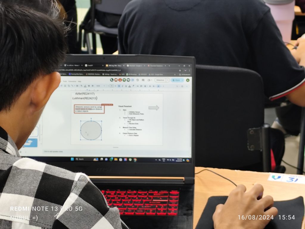
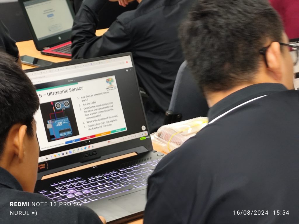
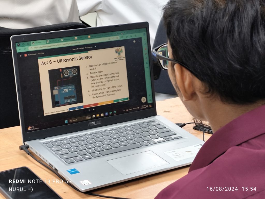
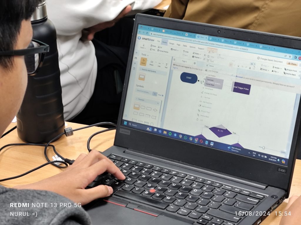
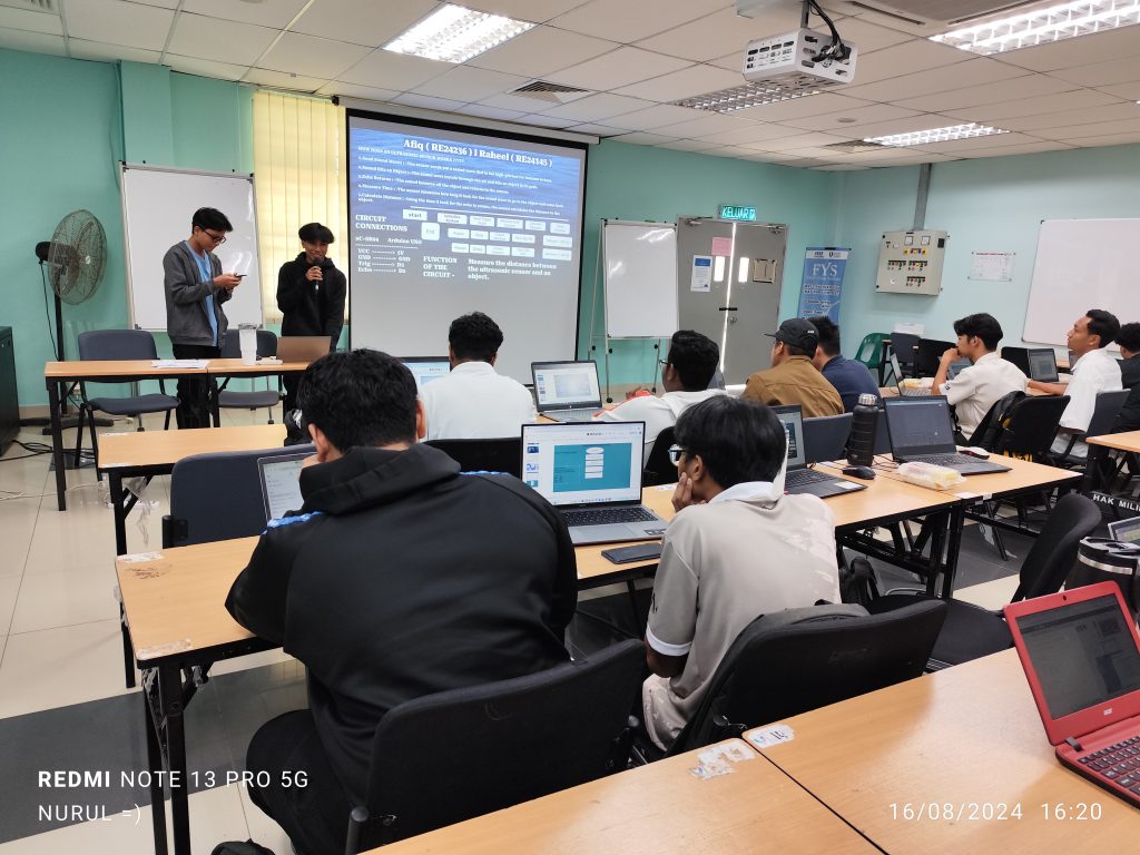
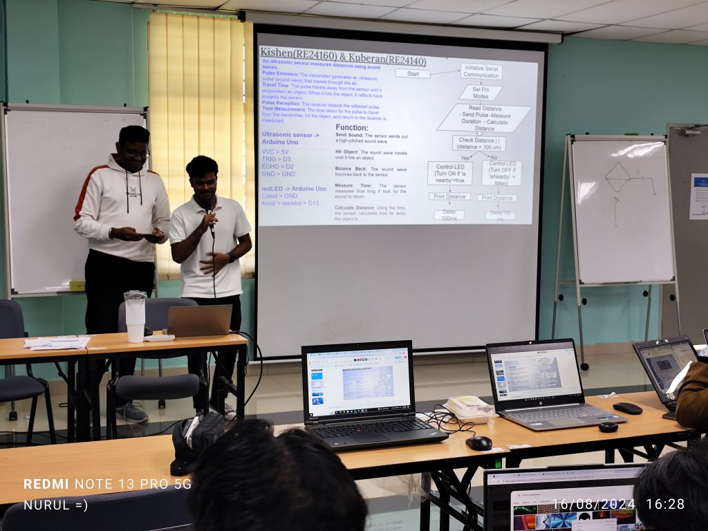
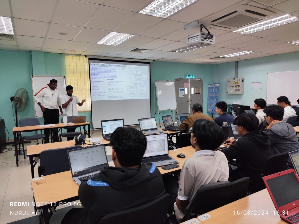
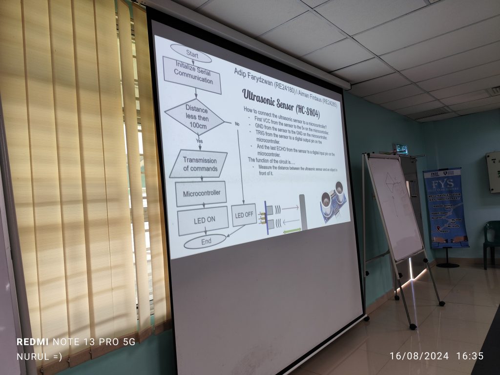
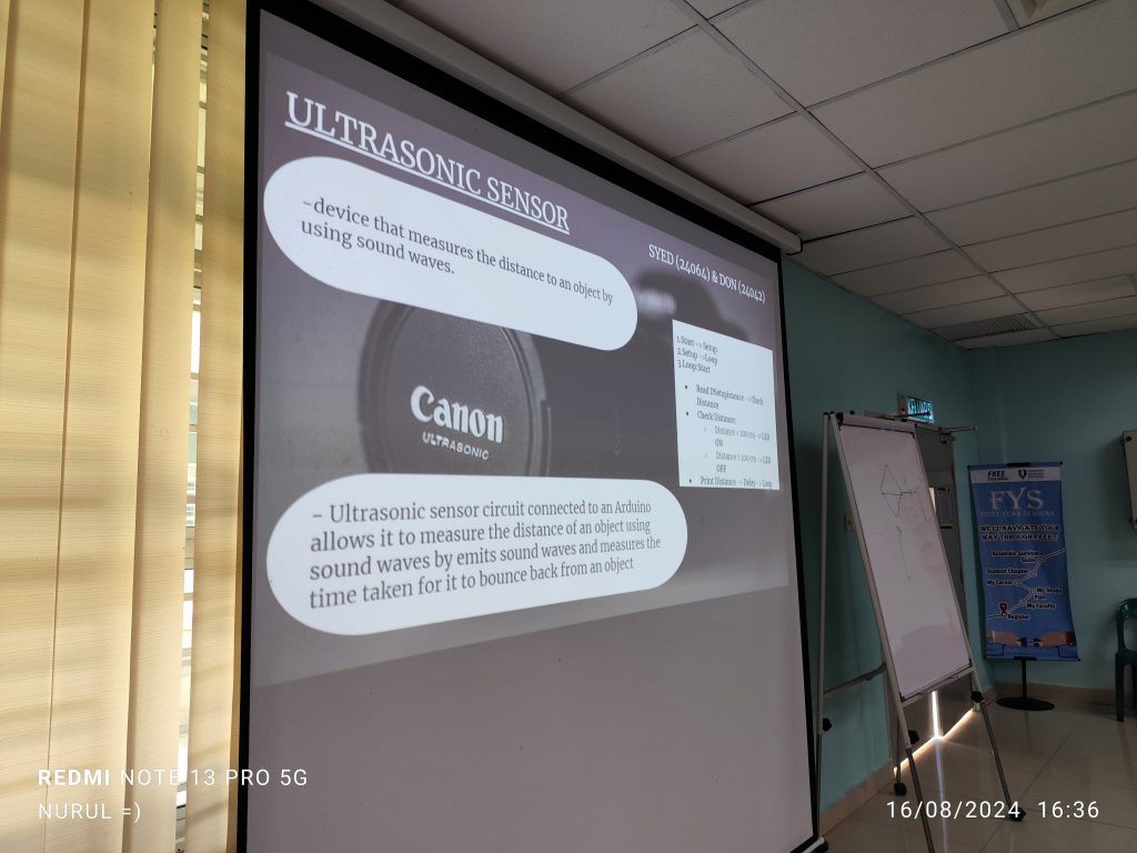
Further advancing their skills, the students used AI-generated code to integrate sensors like photoresistors into their projects, introducing them to the world of analog inputs and sensor data processing. The session culminated in an activity where they used an ultrasonic sensor to measure distance, with real-time results displayed, helping them grasp the concepts of pulse measurement and the practical application of their coding skills in tangible, real-world scenarios.
To all RE students, nice meeting you and hope to see you again in the future.
Nurul – August 17th