Welcome to Week 4 of BHE 3233 and BTE4433. This week marks an important step in your journey as electrical and electronic engineering students, as you begin connecting theoretical concepts with actual hardware implementation. You have now moved beyond just understanding logic on paper—you are starting to build and test real digital systems using Verilog and FPGA tools.
We began the week with a refresher on binary operations, which form the foundation of all digital systems. Understanding how numbers are represented and manipulated in binary is essential, as every digital circuit ultimately operates on combinations of 0s and 1s. From there, we transitioned into describing combinatorial logic using Verilog, focusing specifically on adders.

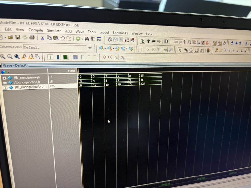
You were first introduced to the half adder, a simple circuit that takes two binary inputs and produces a sum and a carry output. Although basic, it is an important building block in digital design. We then extended this concept to the full adder, which includes a carry-in input, allowing multiple adders to be connected together. This idea of chaining adders is fundamental in designing circuits capable of handling multi-bit arithmetic operations.
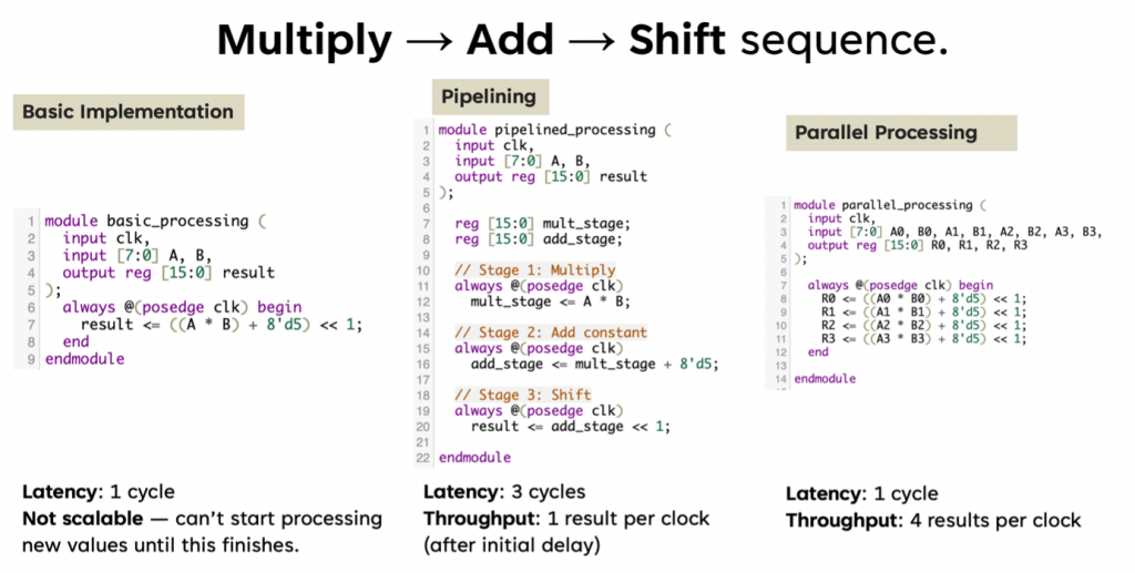
To give you a broader perspective, we briefly explored more advanced adder designs such as the ripple carry adder and the carry look-ahead adder. The ripple carry adder is straightforward but can be slow because each carry must propagate through every stage. In contrast, the carry look-ahead adder improves speed by predicting carry signals in advance, although it comes with increased design complexity. These concepts will become more meaningful as you encounter larger and faster digital systems in the future.


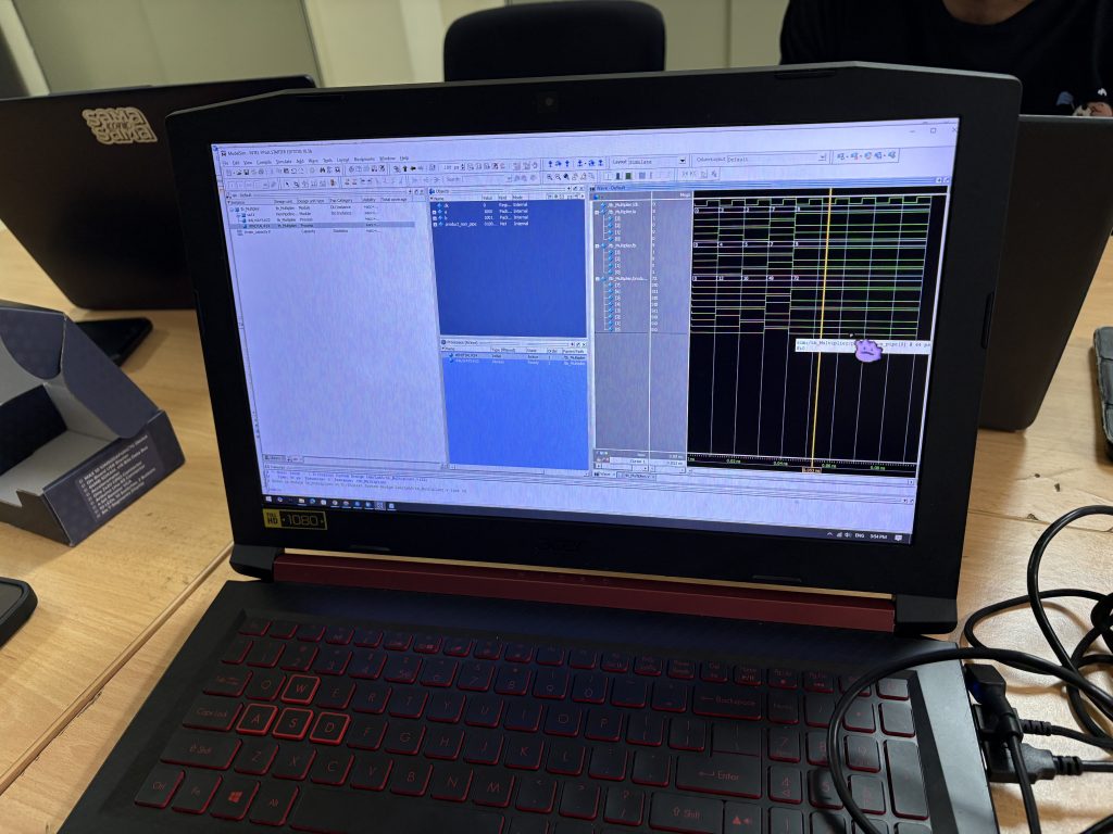
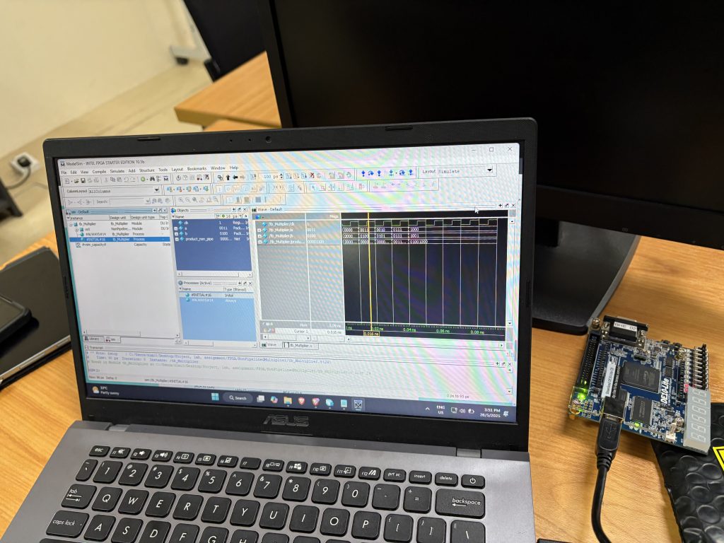
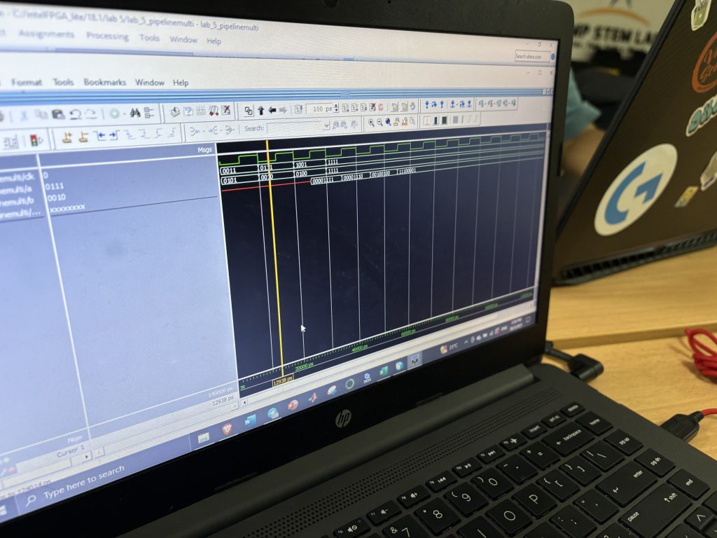
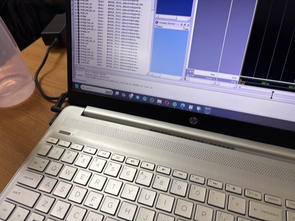
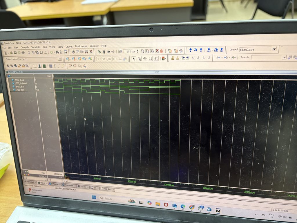
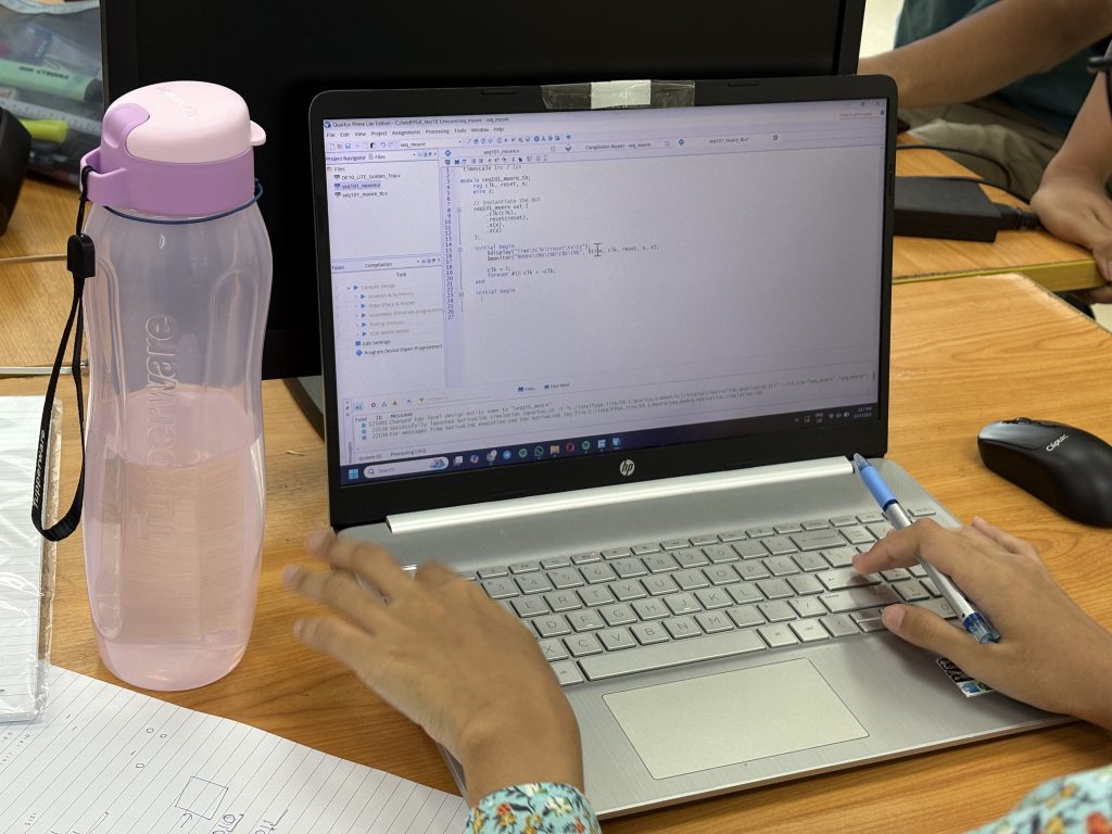
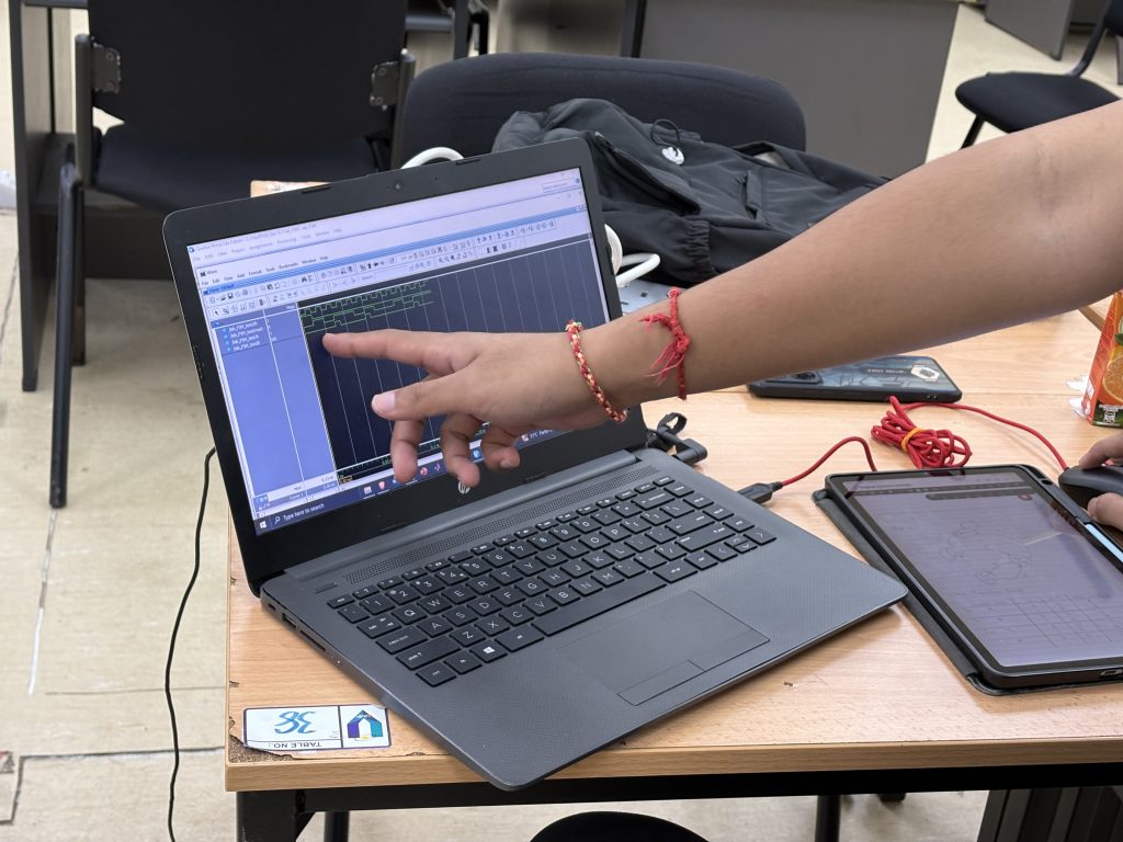
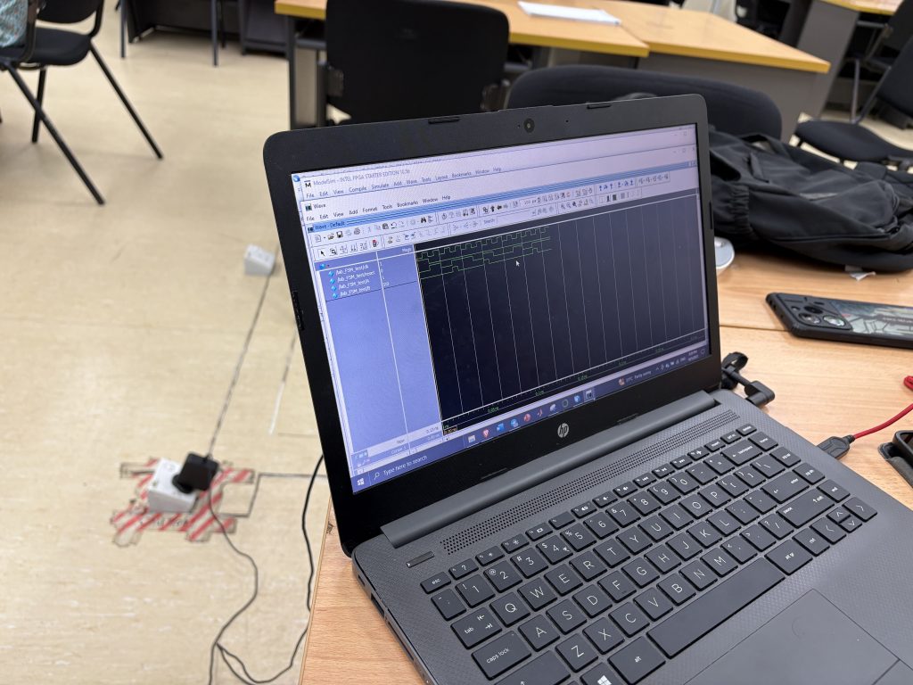
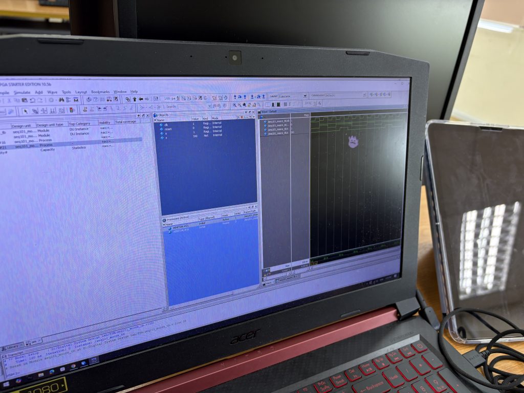
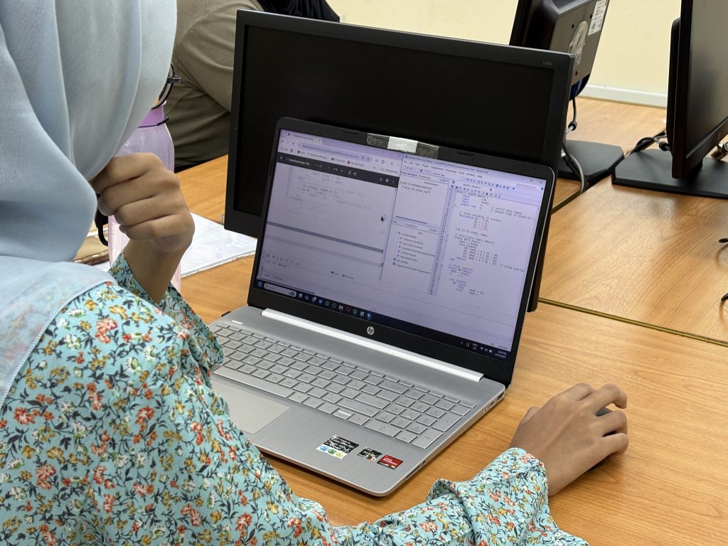
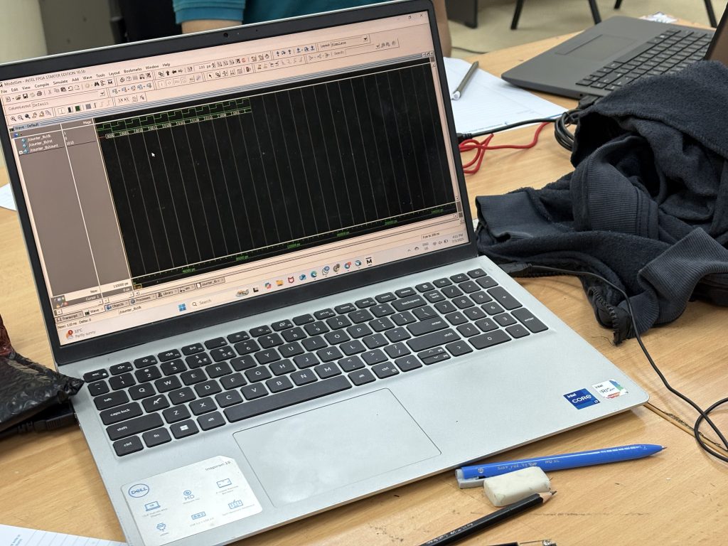
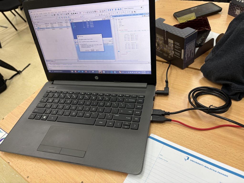
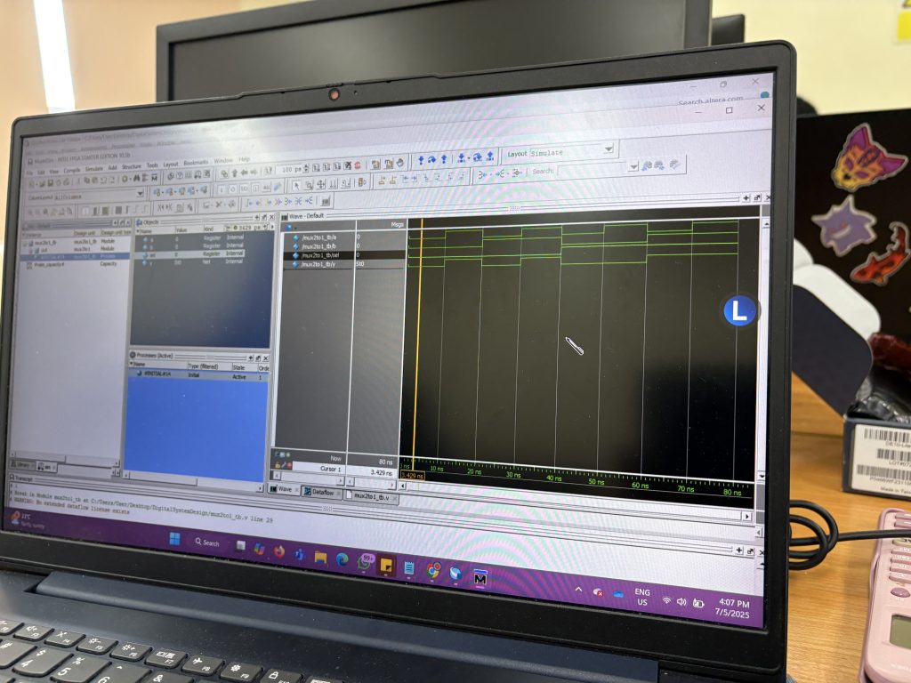
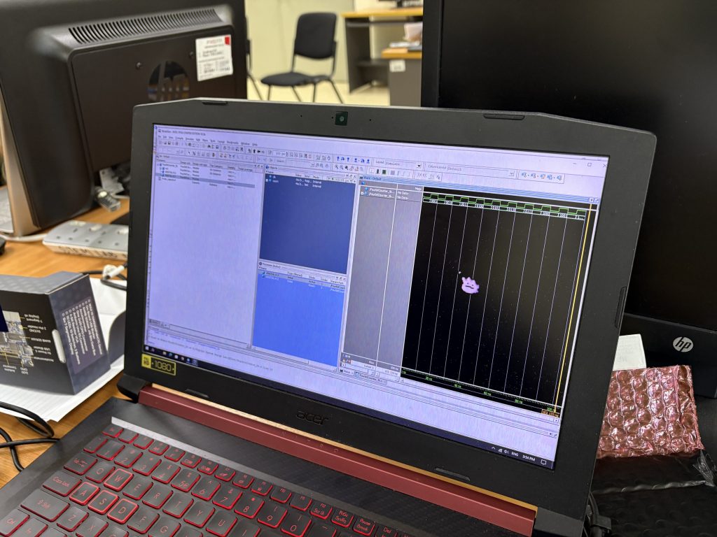
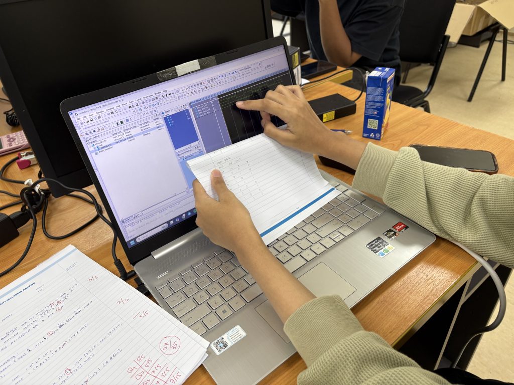
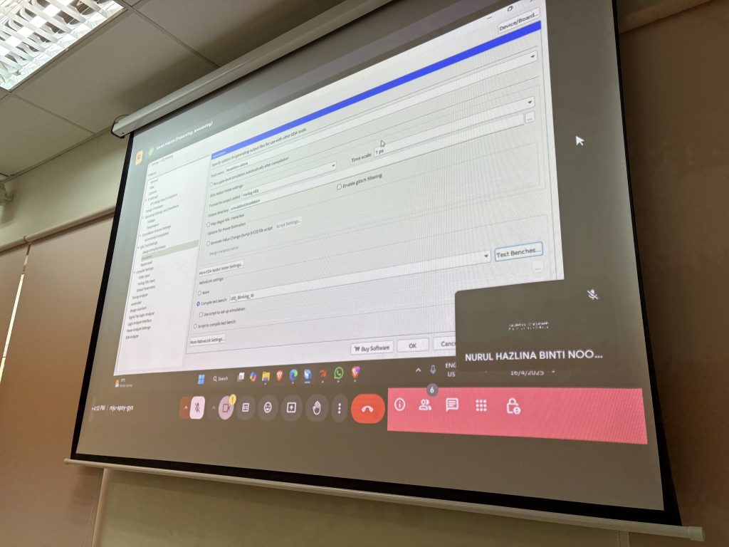
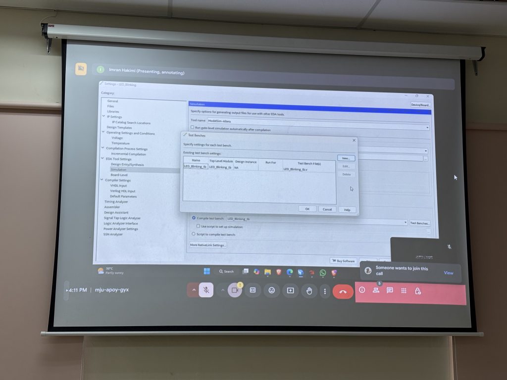
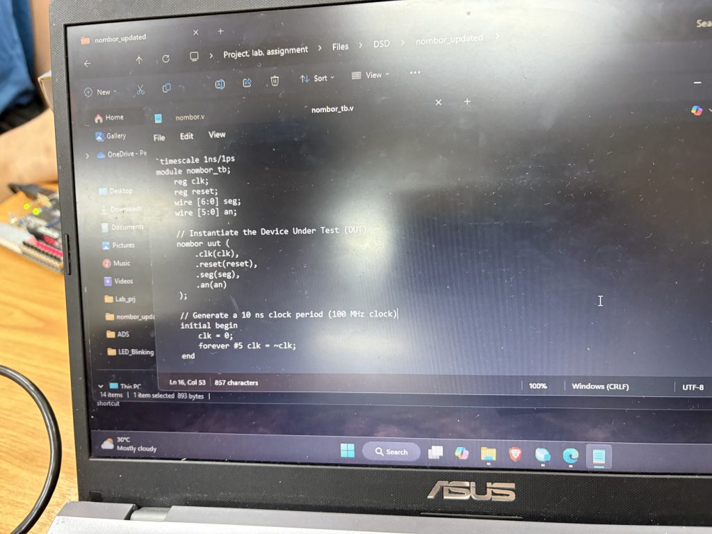
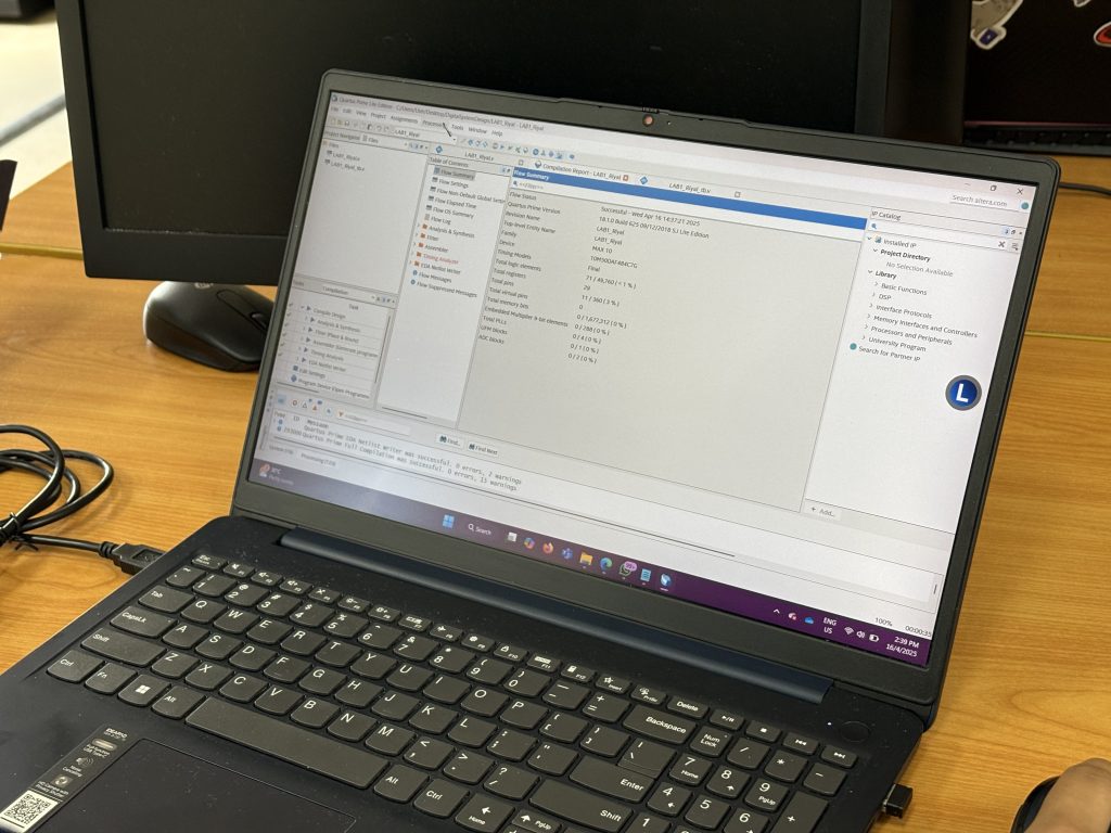
Before moving into Lab 1, we started with Lab 0, which focused on simulation. In this lab, you worked with two files: number.v and number_tb.v. The goal was to simulate your design using ModelSim and observe how digital signals behave over time. This is a critical step in digital design, as simulation allows you to verify correctness before implementing your code on actual hardware.
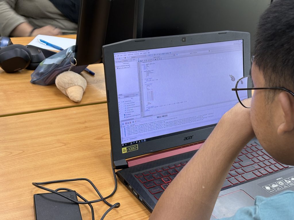
In number.v, you were given a basic up-counter design capable of driving a 7-segment display on the FPGA board. Through this, you explored several important Verilog concepts, including top module declaration, the use of wire data types, and bit buses for representing multi-bit signals. You also examined conditional statements such as if-else, as well as basic mathematical operations within Verilog. By analyzing the waveform output in ModelSim, you were able to see how signals change over time and how your design behaves in response to different inputs. This helped build your understanding of timing and signal relationships in digital circuits.


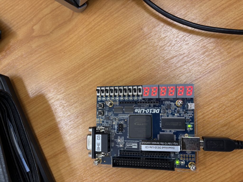
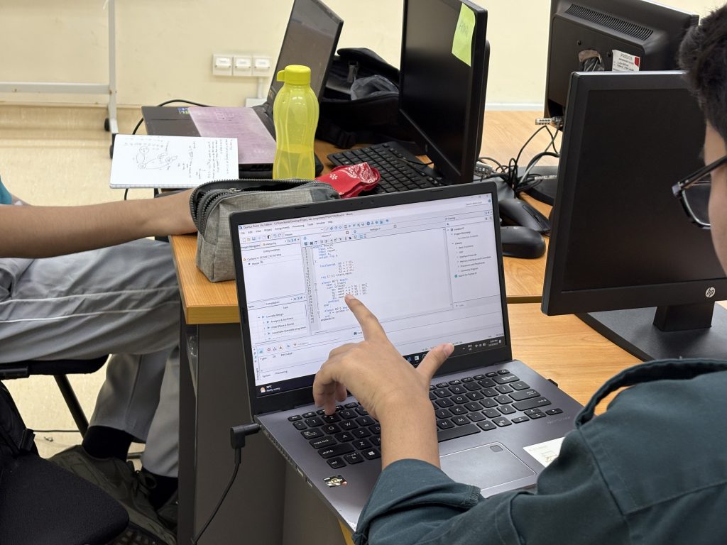
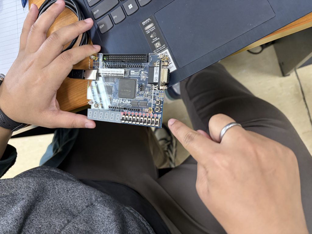
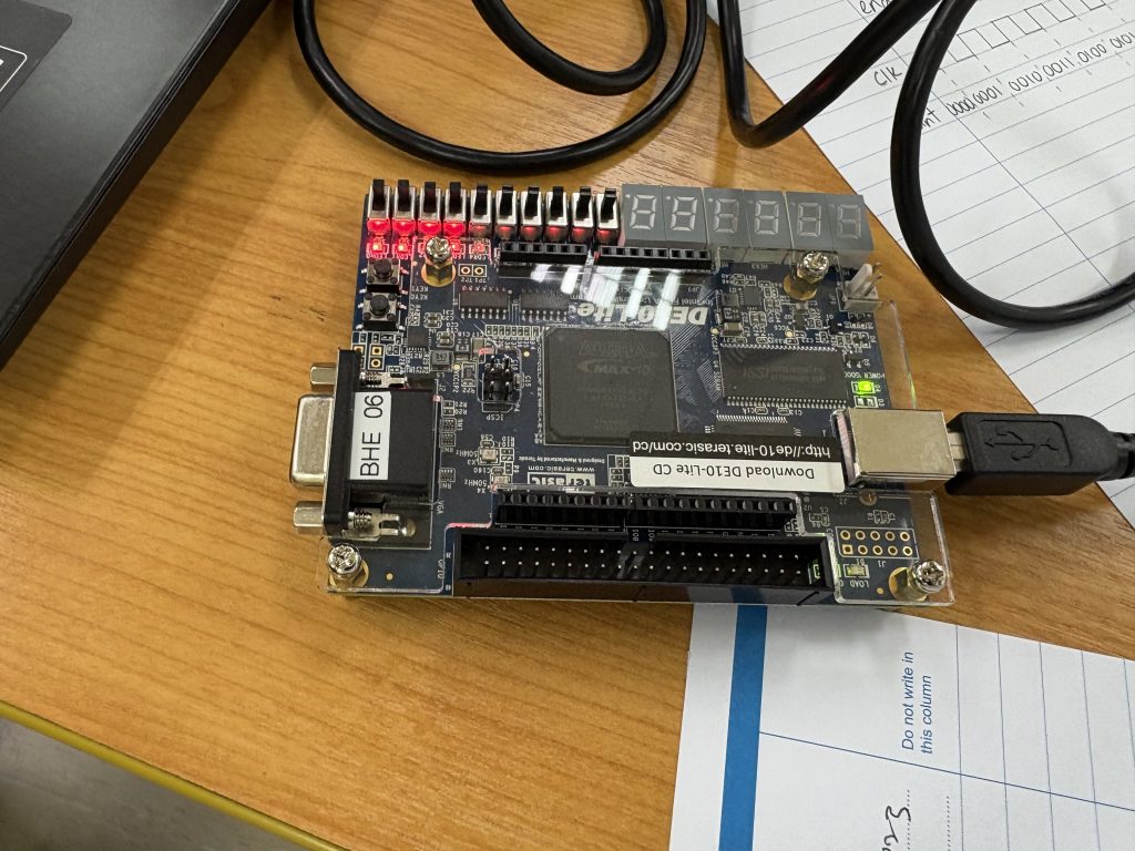
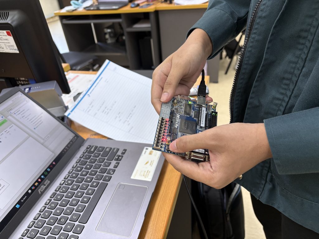
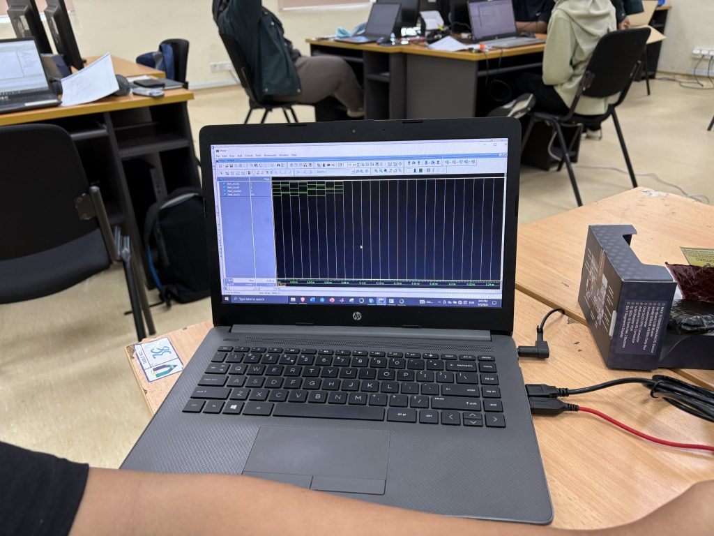
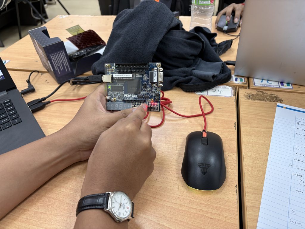
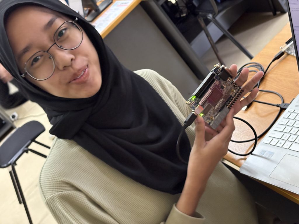
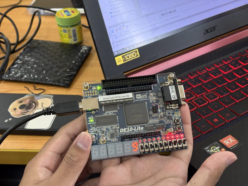
During the Lab 1, which focused on implementing a running LED design on the DE10-Lite FPGA Board. The task required you to write Verilog code, compile it, assign the correct pins for the 10 LEDs on the board, and program the FPGA. The result was a sequence of LEDs lighting up from one end of the board to the other, demonstrating a simple but effective hardware implementation of your design.
This lab was significant because it introduced you to the complete FPGA workflow, from coding to physical output. Many of you experienced the process of compiling your design, resolving errors, performing pin assignments, and finally observing your design working on actual hardware. This transition from simulation to real-world implementation is a key milestone in your learning.

Thank you Lim for the video shot.
Some common challenges were observed during the session, particularly issues with the hardware not being recognized by your computer. In most cases, this was due to problems with the USB-Blaster driver installation. Ensuring that the driver is properly installed and that the device is correctly detected by the system is crucial. Checking the device manager, trying different USB ports, or reinstalling the driver can often resolve these issues.


Overall, this week has equipped you with essential skills in designing combinatorial circuits using Verilog and implementing them on an FPGA platform. You should now have a clearer understanding of how basic arithmetic circuits are built and how digital designs move from code to hardware.
As we move forward, make sure you are comfortable with both your Verilog coding and FPGA setup. The concepts and skills from this week will serve as the foundation for more advanced topics in the coming weeks. If you are still facing issues, especially with hardware setup, it is important to address them early.
See you in Week 5.