BHE3233 – Week 10 – Static Timing Analysis


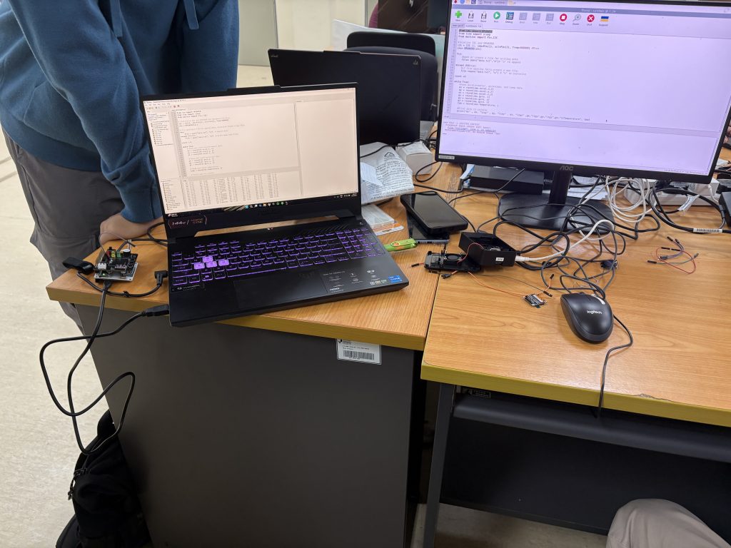
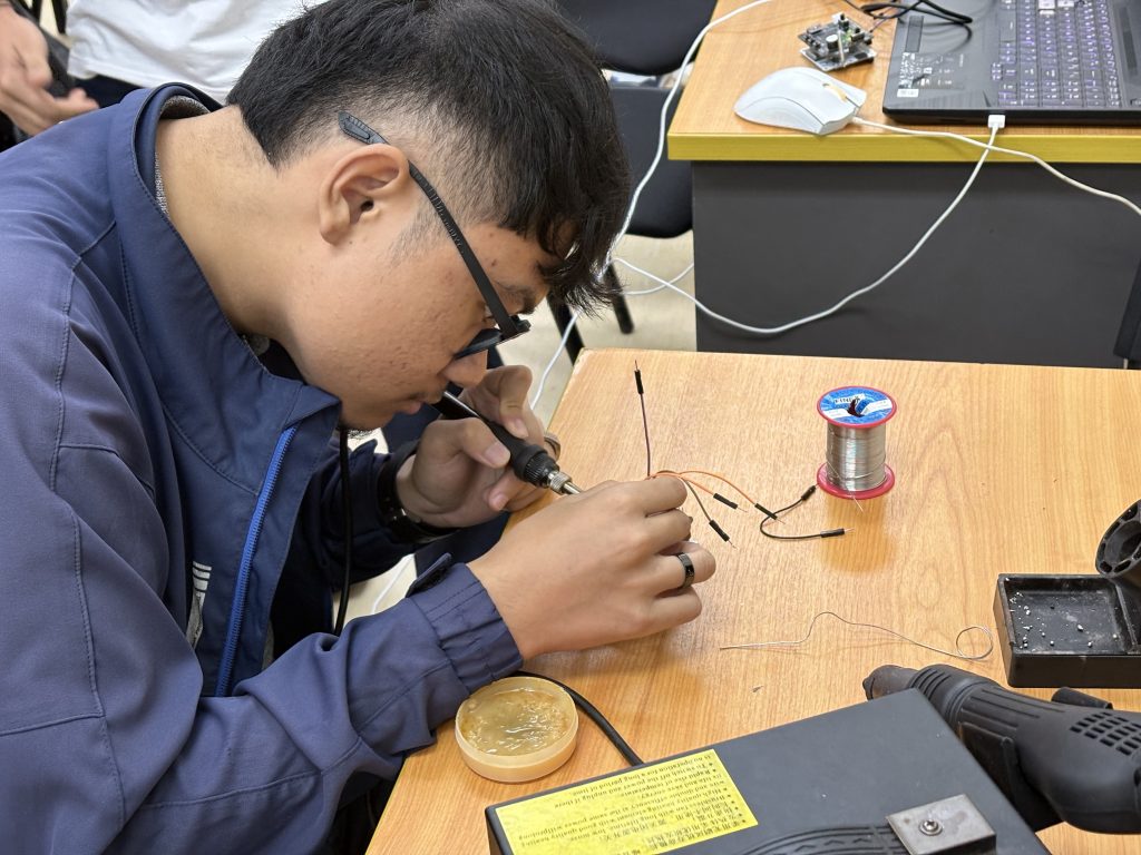
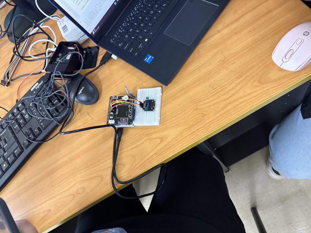
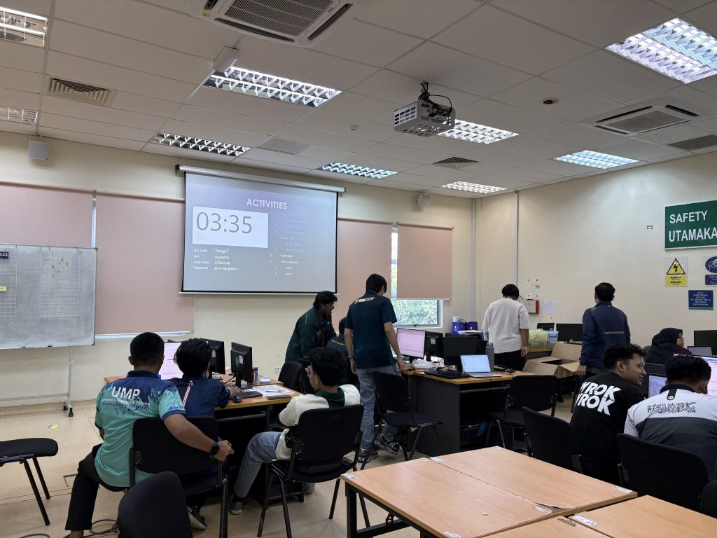
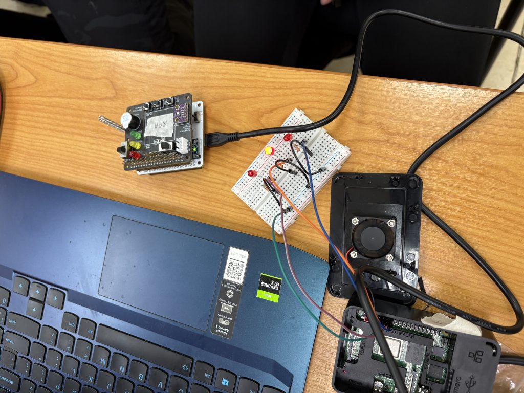
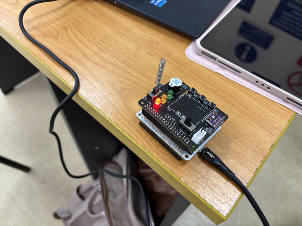
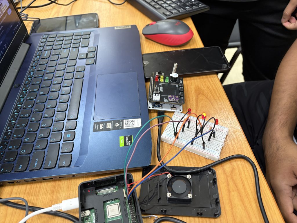
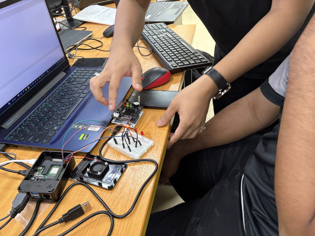
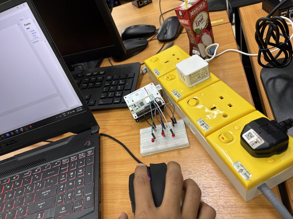
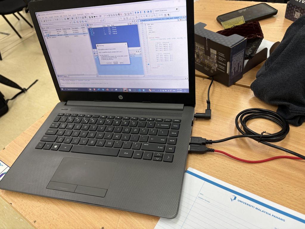
Today we look into one of the most critical yet often overlooked topics in FPGA design – Static Timing Analysis (STA). Understanding STA is key to ensuring that your digital design works not only functionally but also reliably at speed. To ground this theoretical topic, students also completed Lab 5, where they compared pipelined and non-pipelined multipliers and analyzed timing and performance parameters.

What Is Static Timing Analysis?

Static Timing Analysis is a method used to determine if a digital circuit will operate correctly at the target clock frequency without needing simulation input vectors. It uses timing constraints and logic paths to compute:

  • Setup time

  • Hold time

  • Propagation delay

  • Rise and fall times

  • Clock skew

  • Critical path delay

  • Maximum clock frequency

The goal is to verify that all data signals arrive where they need to, on time, under worst-case conditions.

Key Timing Parameters Explained

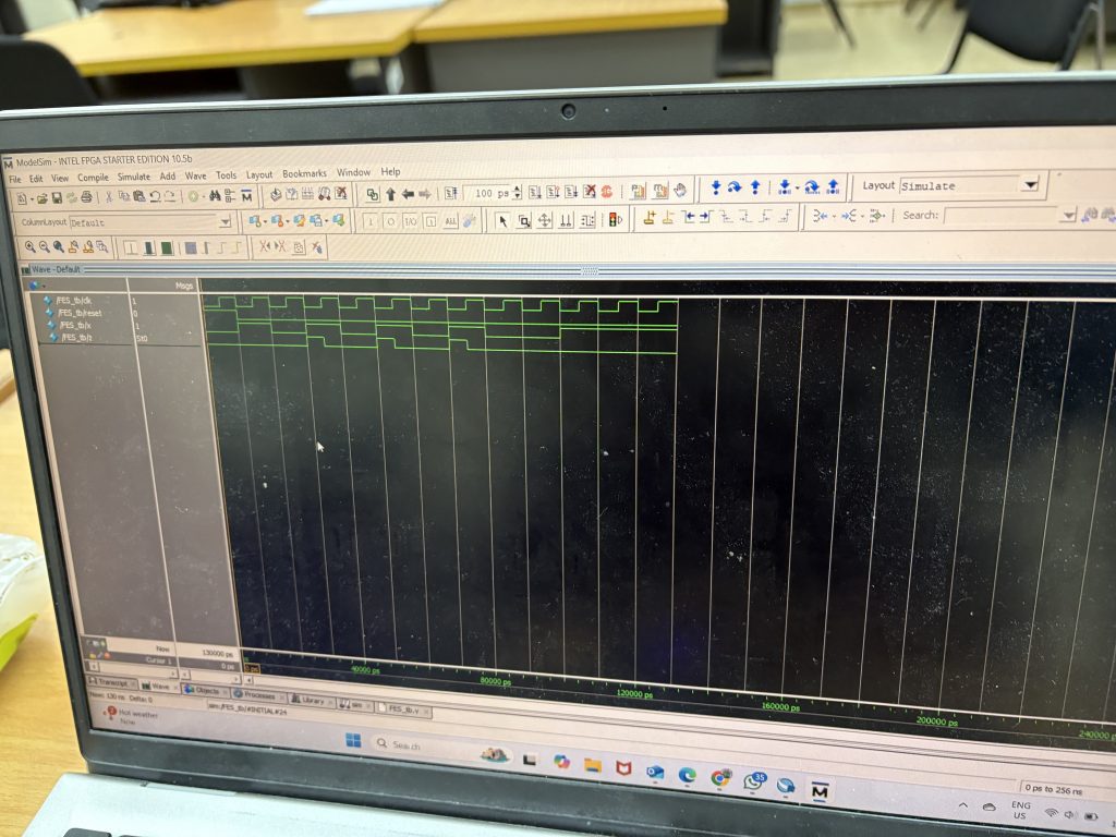
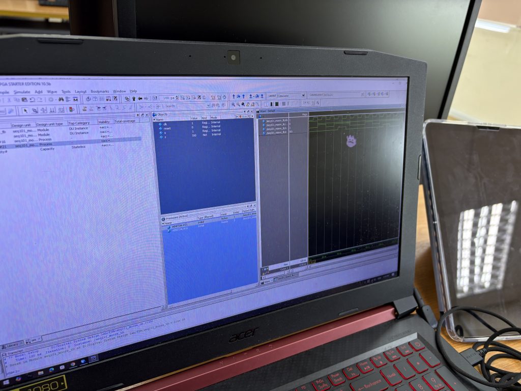
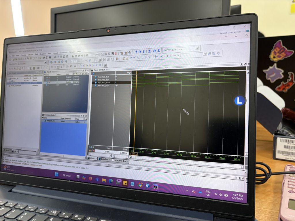
To help visualize the concept, we used a simple design involving two D Flip-Flops (FF1 and FF2) connected through a combinational logic block composed of two logic gates.

1. Setup Time

This is the minimum time the data must be stable before the clock edge arrives at FF2. If violated, data may not be correctly latched.

2. Hold Time

The data must remain stable after the clock edge. If violated, metastability may occur.

3. Propagation Delay

This is the time taken for the signal to travel through the logic gates between FF1 and FF2. It’s dependent on the type and number of gates.

4. Rising/Falling Time

The transition period from low to high or high to low in the signal waveform. Faster transitions are better for minimizing timing uncertainty.

5. Clock Skew

This occurs when the clock arrives at FF1 and FF2 at slightly different times. Clock skew can reduce the effective timing margin.

Example in Class Two Flip-Flops and Logic Path

Imagine a logic path between FF1 (source) and FF2 (destination)

FF1 ----> [AND Gate] ---> [OR Gate] ---> FF2

Let’s assume-

  • Propagation delay through AND = 2ns

  • Propagation delay through OR = 3ns

  • Setup time of FF2 = 1ns

  • Clock skew = 0.5ns

Then, the total delay from FF1 to FF2 is –

2ns (AND) + 3ns (OR) = 5ns

To meet setup time, the clock period must be at least:

arduino
Total delay + Setup time + Skew = 5ns + 1ns + 0.5ns = 6.5ns

This gives a maximum clock frequency of:

1 / 6.5ns ≈ 153.8 MHz

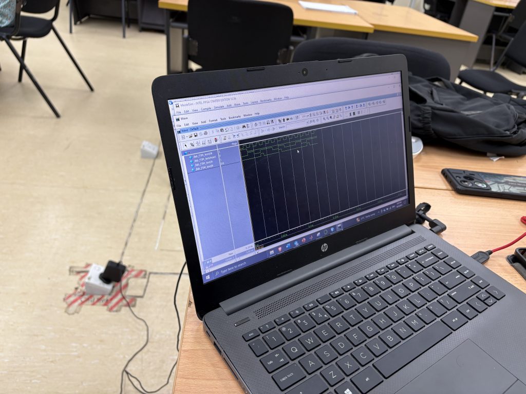
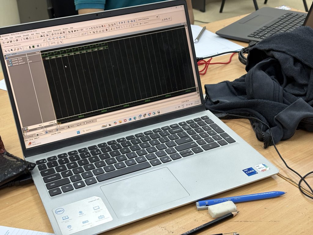
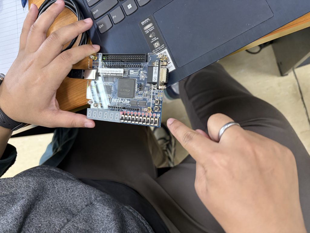
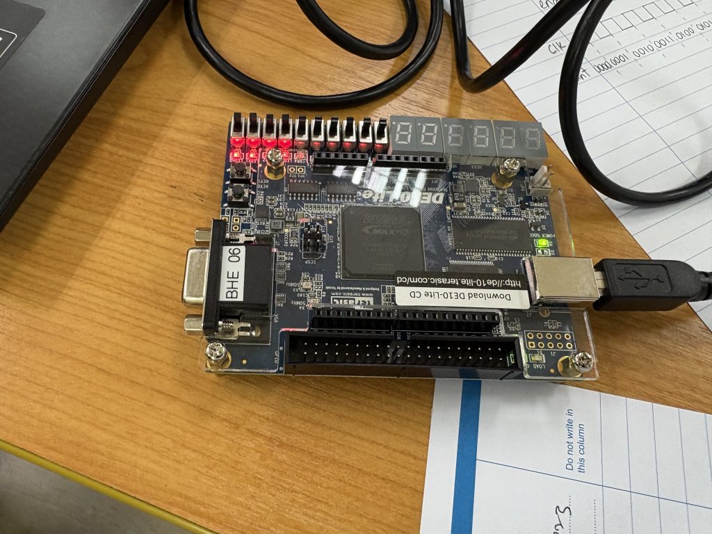
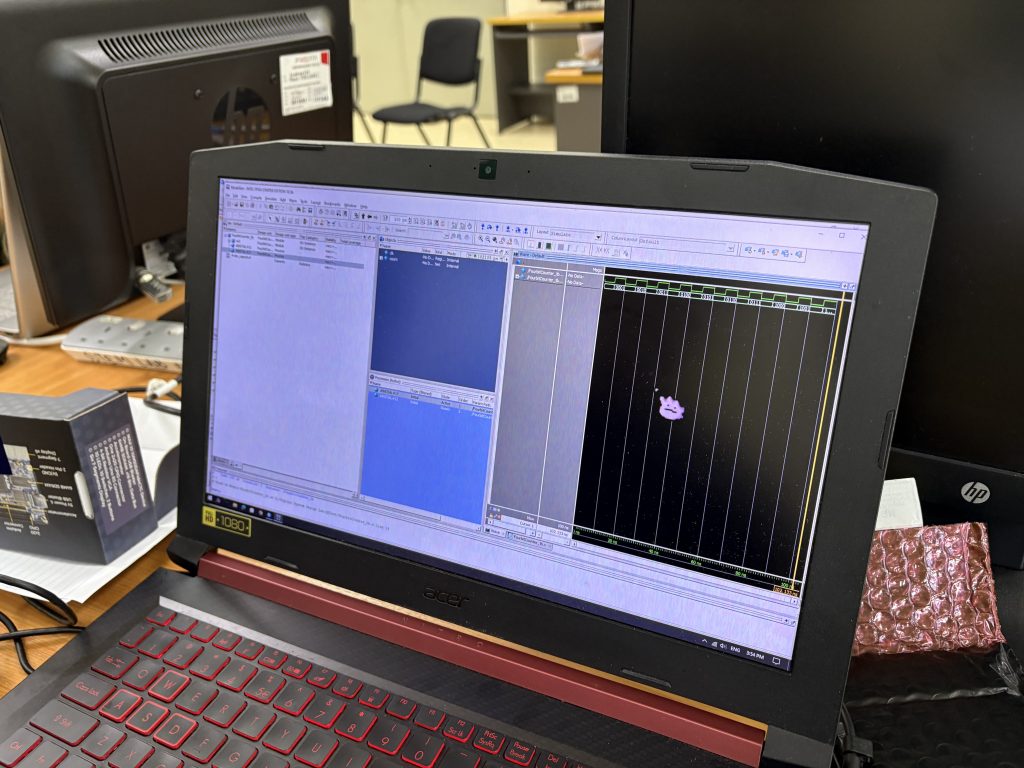
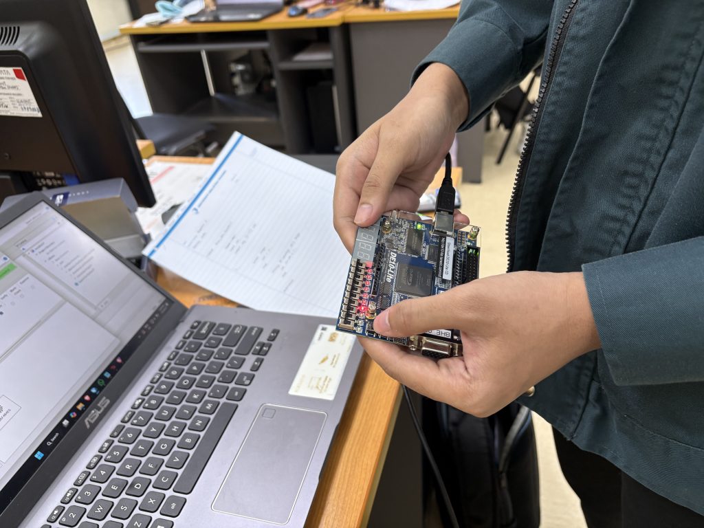
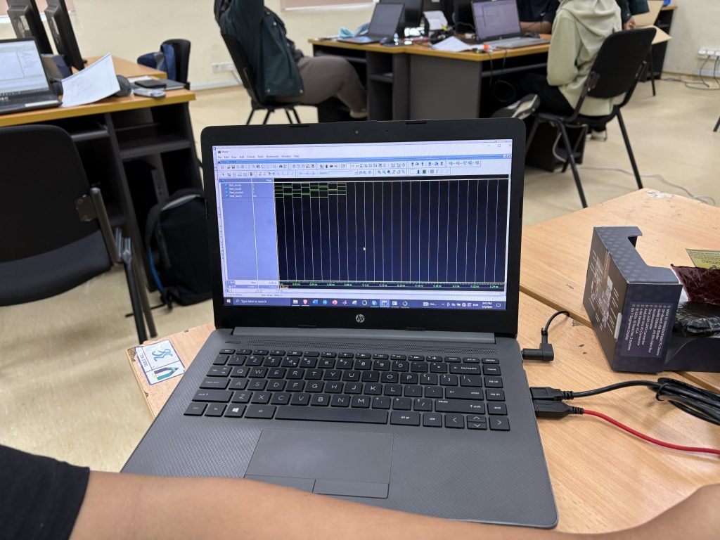
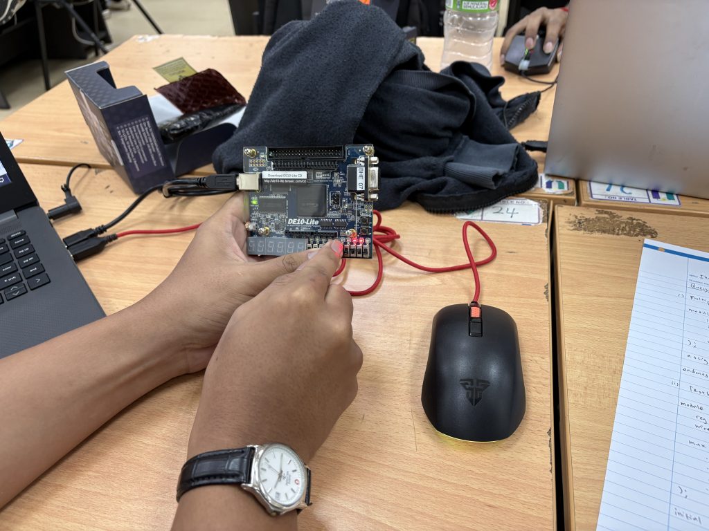
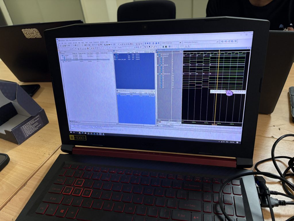
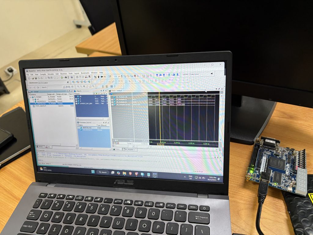
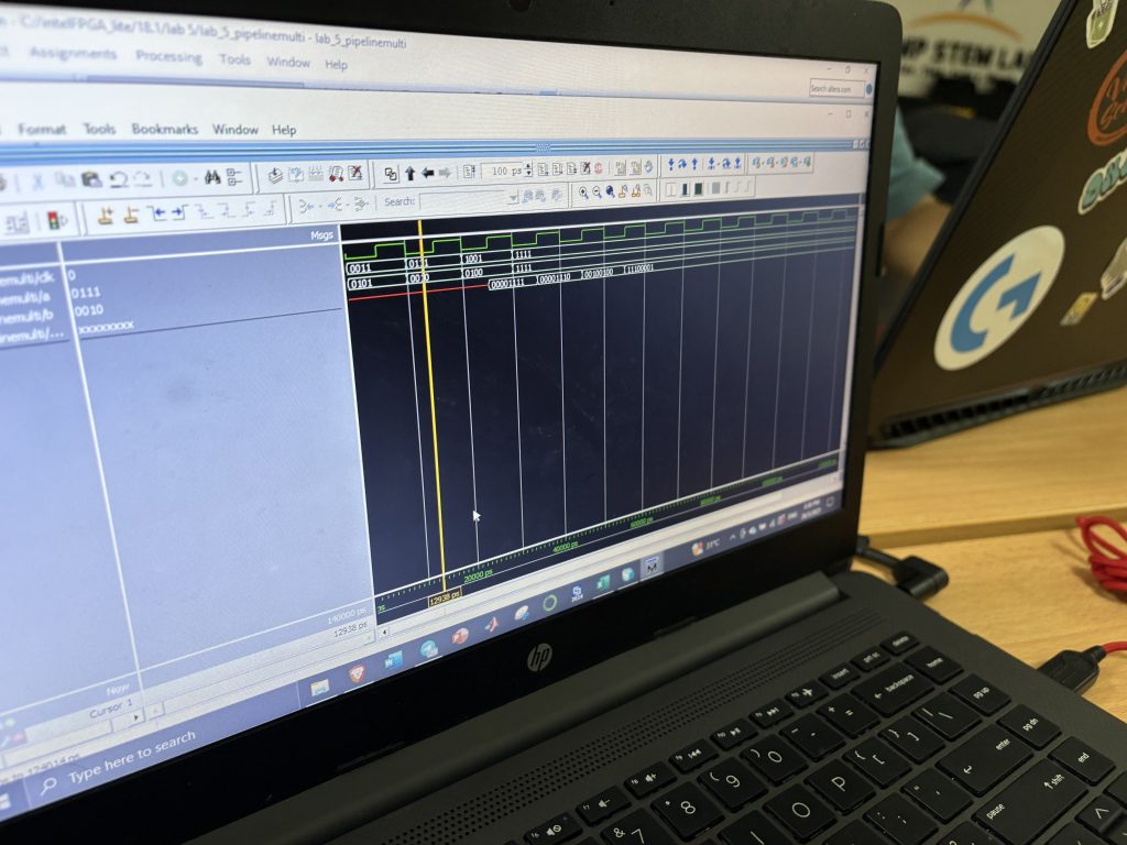
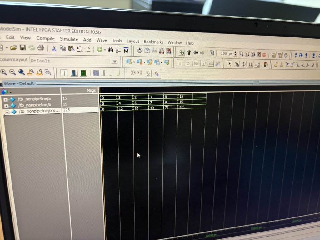
Lab 5 – Pipelining vs Non-Pipelining in Multiplier Design

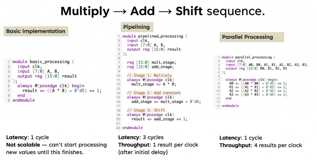
In Lab 5, students implemented and tested two versions of a multiplier:

  • Non-Pipelined Multiplier – Straightforward, all computation happens in one clock cycle.

  • Pipelined Multiplier – Operation split into multiple stages with registers (flip-flops) in between.

They then analyzed the following performance metrics – (hypothetically =))

Parameter Non-Pipelined Pipelined
Critical Path Delay Higher Lower
Max Clock Frequency Lower Higher
FPGA Logic Utilization Lower Higher
Throughput Lower Higher (1 output per cycle after latency)
  • Pipelining reduces the critical path delay, allowing the design to run at a much higher clock frequency.

  • While pipelining increases the logic utilization (more flip-flops), the throughput improves significantly, making it ideal for high-speed applications like real-time data processing in picosatellites or image processing.

  • Static timing analysis helps quantify the improvements, giving insight into real performance beyond just functional correctness.

See you next week for your FPGA project development =)

BHE3233 – Week 9 – Finite State Machine

Today’s class focused on one of the core topics in digital system design—Finite State Machines (FSM)—through an engaging and practical activity: building a 101 sequence detector using a Moore machine.

We began with a recap of FSM fundamentals—specifically the Moore machine, where outputs are solely determined by the current state. This conceptual understanding paved the way for the day’s main activity: designing and testing a sequence detector that identifies the binary pattern 101.

Key areas explored:

  1. State transition diagrams and state encoding

  2. Implementation using case statements

  3. Exploring both dataflow-style FSM and conditional (if-else) statement-based FSMs

  4. Synthesizing and testing using Quartus Prime

Students designed the FSM in Verilog using Quartus. The Moore machine was structured with three states to detect the pattern:

  1. S0 – Initial state

  2. S1 – Received ‘1’

  3. S2 – Received ‘10’

When the full sequence 101 was detected, the FSM output went high.

always @(posedge clk or posedge reset) begin
if (reset)
state <= S0;
else begin
case(state)
S0: state <= (in == 1) ? S1 : S0;
S1: state <= (in == 0) ? S2 : S1;
S2: state <= (in == 1) ? S1 : S0;
endcase
end
end

Simulation and Testbench Creation

To validate the design, students created testbenches that simulated input sequences. Using ModelSim, they:

  • Applied a sequence of 0s and 1s to the in input

  • Monitored state transitions

  • Verified output pulses when 101 was detected

This phase helped students understand the role of simulation in design verification and how FSMs react to clocked inputs in real time.

The case statement simplified FSM implementation, especially when compared to nested conditional (if-else) logic. They also discussed how a well-structured FSM can lead to clean, readable, and maintainable RTL code—an essential practice in real-world design.

Learning Outcomes

By the end of the session, students were able to:

  1. Describe and implement Moore FSMs in Verilog

  2. Translate a sequence detection problem into state transitions

  3. Use Quartus for synthesis and ModelSim for simulation

  4. Compare dataflow FSM vs. conditional FSM modeling

BTE1522 Week 9 Working with Sensors

This week brought us deeper into the world of physical computing as we explored the integration of two essential sensors: the OLED SSD1306 display and the MPU6050 accelerometer-gyroscope module. This hands-on session emphasized how different devices communicate with a microcontroller, helping students solidify their understanding of communication protocols and library dependencies—two vital concepts in embedded systems development.

Part 1: Getting Started with the OLED SSD1306

We kicked off the session by working with the OLED SSD1306, a compact I2C display module. The key learning outcomes from this segment included:

  • Understanding I2C protocol and how to enable it on Raspberry Pi.

  • Installing the Adafruit CircuitPython SSD1306 and Pillow libraries.

  • Writing and modifying Python scripts to display text such as “Hello” and “MicroPython” on the screen.

  • Recognizing how display buffers work in conjunction with ImageDraw and ImageFont.

This gave students the confidence to interact with a visual output device and understand how pixel-based rendering works in Python.

Part 2: Reading Motion Data with MPU6050

Next, we connected the MPU6050, a 6-axis motion sensor capable of detecting acceleration and angular velocity. Students worked through:

  • Wiring the MPU6050 module correctly using the I2C pins.

  • Installing and using the mpu6050 Python library (or equivalent like smbus and i2cdev depending on setup).

  • Writing code to retrieve:

    • 3-axis accelerometer data (accel_x, accel_y, accel_z)

    • 3-axis gyroscope data (gyro_x, gyro_y, gyro_z)

    • Temperature reading

This activity allowed students to appreciate how raw sensor data can be captured, processed, and used to build context-aware applications like motion-based controls or orientation tracking.

Throughout the session, students faced challenges such as installing the correct libraries, identifying I2C addresses using i2cdetect, and debugging I2C communication issues. These challenges were treated as learning opportunities that mimic real-world embedded systems development.

By the end of the class, students were able to:

  • Display custom messages on an OLED screen.

  • Capture and print real-time motion data from the MPU6050 sensor.

  • Understand how communication protocols (I2C) function in real applications.

  • Connect theory with practice through experiential learning.

Today’s activities not only strengthened students’ coding and hardware integration skills but also encouraged logical troubleshooting, critical thinking, and problem-solving—all key aspects of becoming a proficient developer. We’re building toward more advanced sensor-based projects in the coming weeks, and this session laid an excellent foundation.

As always, proud of the students’ persistence and teamwork as they explored and completed the activities.

BTE1522 – Week 8 – Raspberry Pi Programming

This week, we kicked off with Microcredential 2 and 3 focusing on hands-on Raspberry Pi segment

We started off with the fundamentals – configuring the Raspberry Pi environment. Students explored the process of setting up the Raspberry Pi 4, learning how to boot the system, OS installation, update packages, and enable interfaces like SSH and I2C. This step was crucial to ensure their boards were fully prepared for the upcoming hardware experiments.

MC 2 – Chapter 1 -5 Raspberry Pi Installation and Setting Up

Alongside this, we discussed key differences between Raspberry Pi 4 (a microprocessor-based platform) and Raspberry Pi Pico (a microcontroller-based platform). This opened up meaningful discussions on the architecture, applications, and performance of both systems.

MC 3 – Chapter 1 & 2: Hardware Warm-Up Activities

The class then moved into Microcredential 3, tackling Chapter 1 and Chapter 2, which introduced basic hardware control using Python and MicroPython. Over these two chapters, students completed four practical activities:

  1. Lighting up an LED (Act 1) – their very first GPIO output!

  2. LED Blinking (Act 2) – introducing timing and control loops.

  3. Reading Digital Input with Push Button (Act 3) – detecting user input via GPIO.

  4. Push Button to Control LED (Act 4) – combining input and output for basic interaction.

These warm-up activities weren’t just about turning lights on and off. They were designed to help students:

  1. Compare Python 3 (used on Pi 4) vs MicroPython (used on Pico).

  2. Understand how different hardware platforms influence programming paradigms.

  3. Build a mental model of how microprocessors and microcontrollers handle digital I/O.

Learning Through Doing

At UMPSA STEM Lab, we strongly believe in embodied learning – and this week was a great reflection of that. Students didn’t just hear about hardware or programming; they wired it, coded it, debugged it, and saw the immediate outcome of their logic and effort. It was beautiful to see LEDs blinking and eyes lighting up in sync.

Next week, we’ll continue building on this foundation by introducing OLED displays and sensor integration — more advanced interactions await!

Btw sharing with you the production of Rasp Pi in their facilities in the UK:-

Congratulations Dr Nurulfadzilah Hassan

Nurulfadzilah did her PhD research in developing a novel composite – Epoxy Barium Titanate for the use of microstrip  patch antenna design. In this work she explored and characterized BTo targeting for application in 2.4 GHz antenna.

With 6 publications throughout the research, she successfully defended her thesis with minor revision required.

Congratulations once again.