


The world is digital, but life is analog..
It’s project time =)
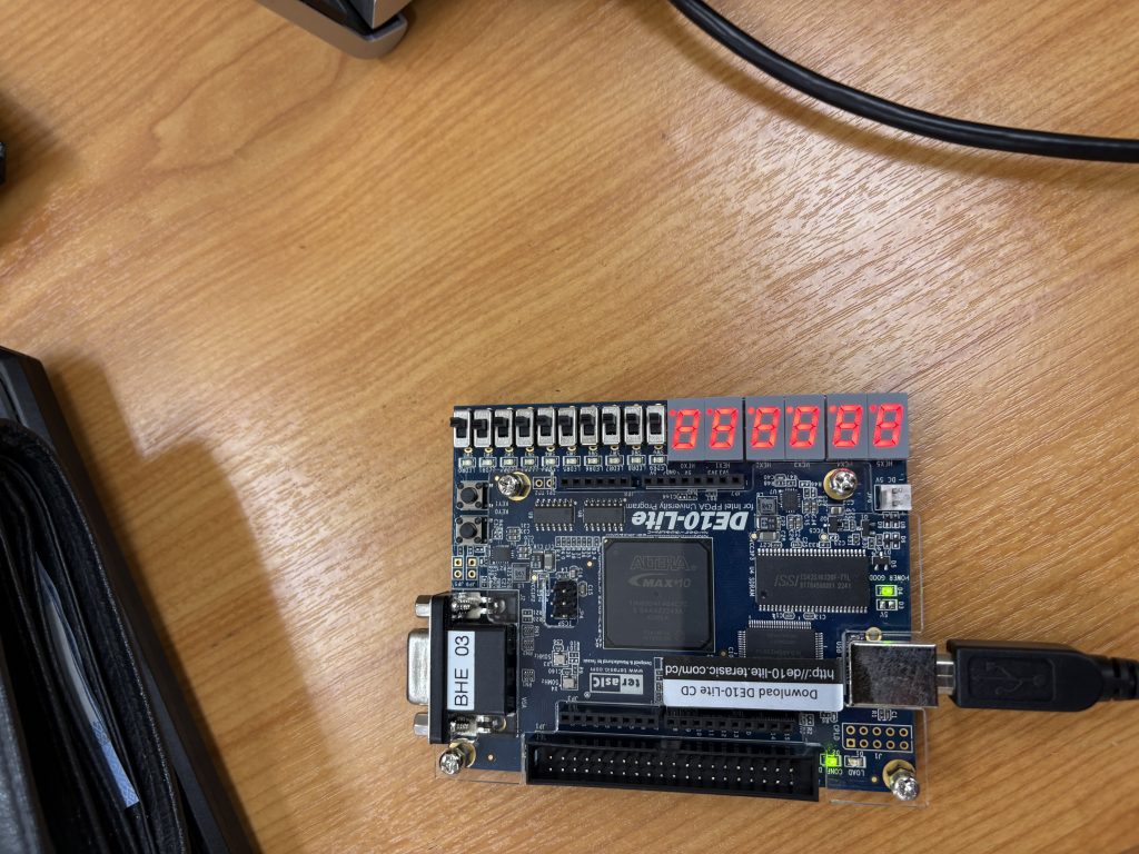
This semester in BHE3233 – Digital System Design, we’re exploring practical world of digital hardware by implementing real-time, embedded digital systems using the DE10-Lite FPGA board. Building on the fundamentals of Verilog, FSMs, and RTL design we’ve covered, students now have the opportunity to apply their knowledge through these exciting hands-on projects. Each project emphasizes different aspects of digital design—from FSM sequencing to pipelining and datapath architecture.
These projects were carefully curated to cover a wide range of course outcomes, from combinational and sequential logic design to system-level implementation using FSMs and RTL pipelines. Students not only reinforce theoretical understanding but also gain confidence in developing real-time FPGA applications using Verilog on the DE10-Lite board.
Before jumping into their projects, the students have already completed structured labs covering:-
FSM design and simulation
RTL pipelining
Clocking and timing constraints
Static timing analysis
7-segment display interfacing
Debouncing and switch inputs
These foundational skills are directly applicable to the project implementations.
Here’s a detailed look at the 6 project titles offered this semester:-
1. Morse Code Encoder and LED Blinker
Objective – Design a finite state machine (FSM)-based system that converts input characters (A-Z, 0-9) into Morse code and blinks an LED accordingly.
Key Features –
Input a hardcoded message (or via DIP switches)
FSM handles character-to-Morse conversion (dot and dash)
LED blinks in Morse timing format
Optional – Display current character on a 7-segment display during encoding
Learning Outcomes – FSM design, output timing control, sequential logic, user interaction.
2. Basic 8-bit RISC CPU Implementation
Objective – Build a basic 8-bit CPU that supports core instructions such as ADD, SUB, LOAD, STORE, and JMP.
Key Features –
4 to 8 general-purpose registers
Instruction decoder and ALU unit
ROM-based instruction memory and RAM-based data storage
Output status or values via LEDs or 7-segment display
Learning Outcomes – Datapath design, FSM for control unit, memory interfacing, and simple instruction architecture.
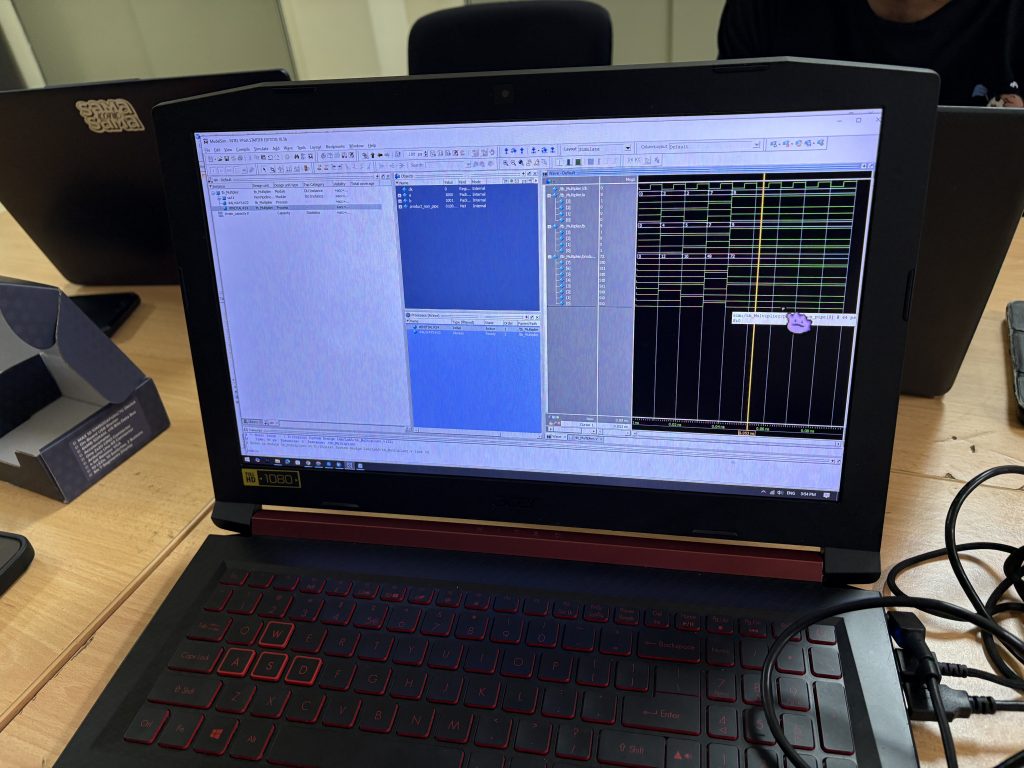
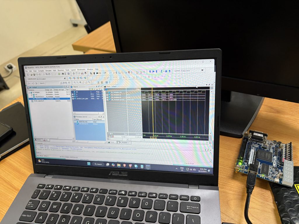
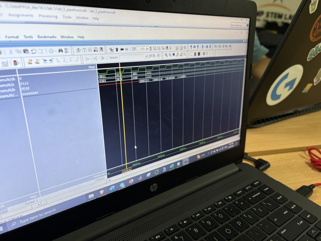
3. Parallel Multiplier Using RTL Pipelining
Objective – Design a high-speed 8-bit parallel multiplier using RTL pipelining techniques.
Key Features –
Inputs via DIP switches or pushbuttons
Multi-stage pipelining of partial products
Output result on 7-segment displays
Compare pipelined design with pure combinational multiplier in terms of:-
Critical path delay
Maximum clock frequency
FPGA logic utilization
Throughput
Learning Outcomes – Pipelined architecture, latency vs. throughput, performance analysis.
4. Digital Stopwatch with Lap Function
Objective – Create a stopwatch with basic timing functions and lap time capture.
Key Features:
Start/Stop/Reset controls via pushbuttons
FSM-based timing logic
4-digit multiplexed 7-segment display
Capture and display lap time on button press
Learning Outcomes – Sequential system design, timing counters, 7-segment multiplexing, user interface design.
Objective – Develop a digital locking system with password protection using FSM.
Key Features –
User password entry via DIP switches
Status feedback through LEDs or 7-segment
Lock/unlock logic with real-time comparison
Optional: Add retry limit and lockout on failed attempts
Learning Outcomes – FSM logic, comparison algorithms using shift registers, and embedded security logic.
6. Dice Game Controller
Objective – Simulate a simple 2-player dice game with visual feedback and turn-based logic.
Key Features –
Pushbutton to initiate dice roll
Use LFSR (Linear Feedback Shift Register) to generate pseudo-random numbers (1–6)
Output displayed using 7-segment or LED
FSM handles player turns and win conditions
Learning Outcomes – Random number generation using LFSR, FSM game logic, 7-segment display control.
Today, each group presented their project progress. Well done!
Functional demo on the DE10-Lite board
Timing and performance analysis
Challenges and solutions in design
Looking forward to final outcome and submission in Kalam!

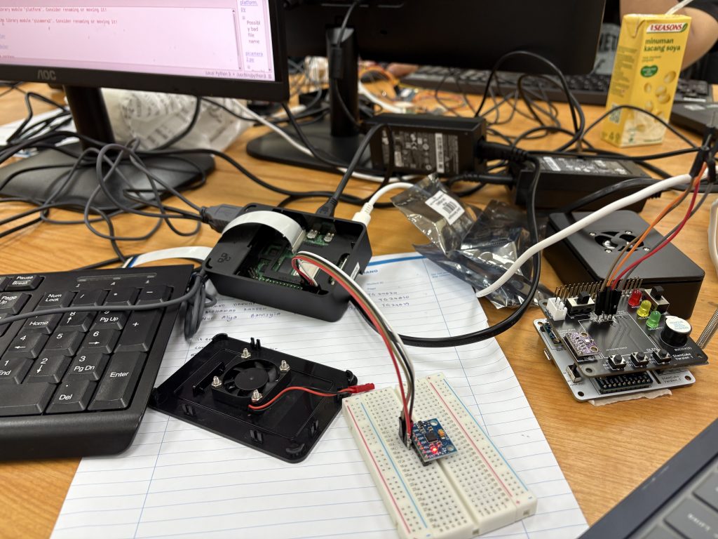
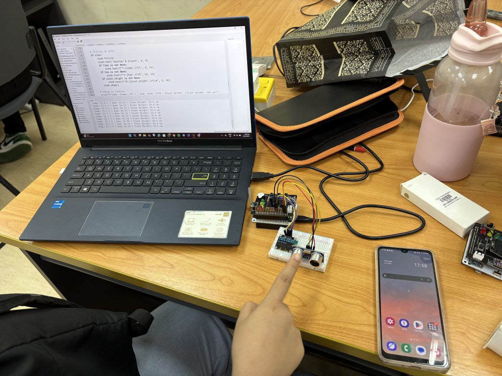
Over the past three weeks, our BTE1522 class transitioned into full project-based learning mode, where students were tasked to apply all they have learned throughout the semester—from Python programming basics to hardware interfacing with the Raspberry Pi 4. This phase was not just about completing an assignment—it was about creating functional, working solutions from scratch.
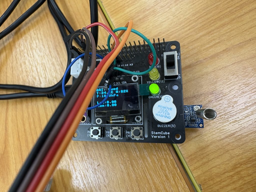
Each group (consisting of three students) was equipped with:
A UMPSA STEM Cube
Raspberry Pi 4
Camera Module
GPS Sensor
BME280 (temperature, humidity, pressure)
MPU6050 (accelerometer and gyroscope)
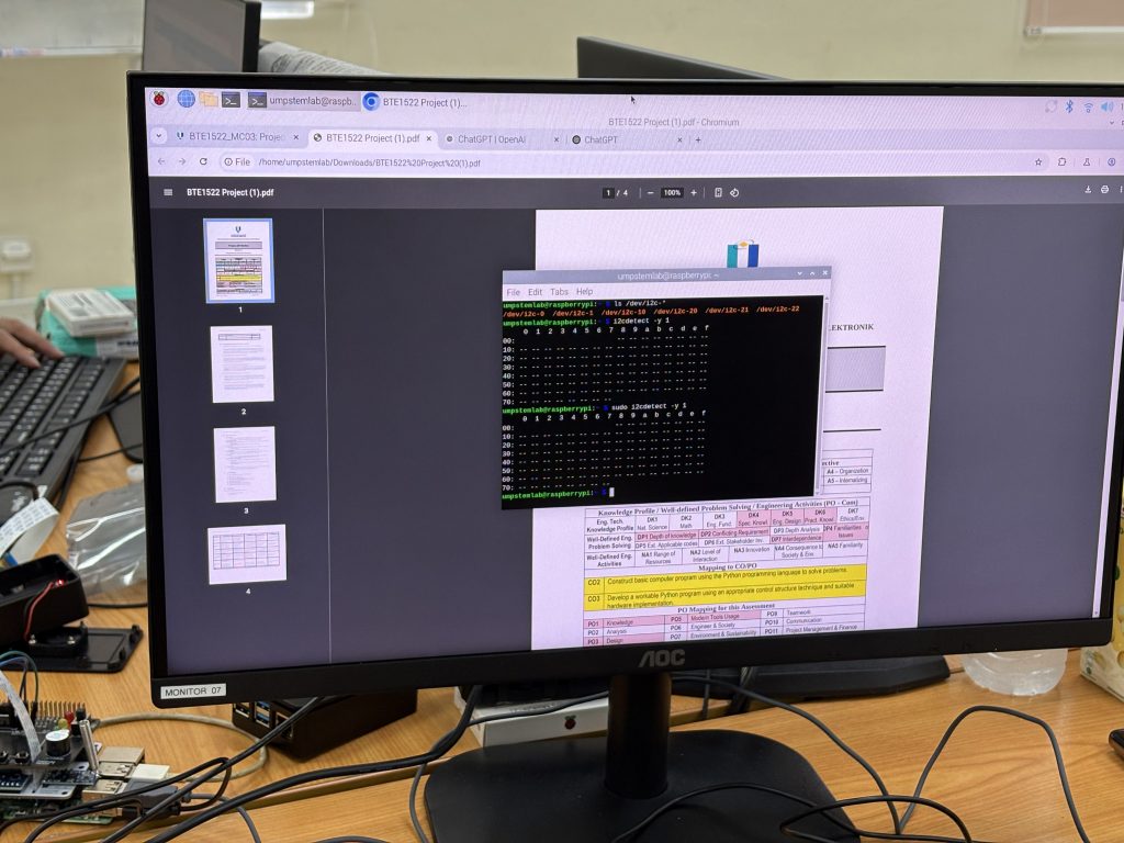
Students selected one topic from a set of project assignments, all of which required multidisciplinary skills. Each project had to include the following components:
Sensor Integration: Establish working connections between Raspberry Pi and the sensors.
Data Storage: Build a working database—either local (e.g., SQLite) or cloud-based (e.g., Firebase, Google Sheets).
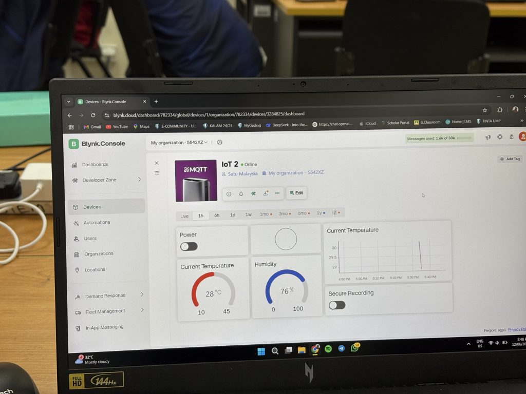
Dashboard Development: Create a working user interface/dashboard using tools like Streamlit, Flask, Adafruit IO, or Blynk to visualize data and system status.
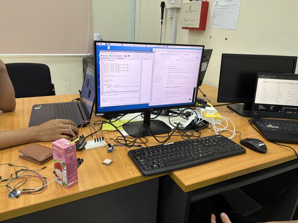
The Learning Process
This phase was entirely project-based, meaning students were expected to learn through experimentation, debugging, and problem-solving. Unlike guided tutorials, this process encouraged independent learning and collaboration:
Debugging wiring errors
Fixing Python runtime bugs
Reading sensor data accurately
Sending and retrieving data from a database
Building interactive visual dashboards
Learning programming—especially physical computing—is most effective when you’re actually doing it. The moment something doesn’t work, and you have to troubleshoot, is when you truly begin to understand what you’re building. the most important thing is NOT TO GIVE UP 🙂
This project based learning phase is aimed at solidifying concepts from earlier weeks, including:
Python functions and loops
Conditional logic
File and data handling
Sensor reading and real-time feedback
REST APIs and interface design
Final Submission Checklist
As the project phase concludes, students are required to submit their work via KALAM. Each group should prepare:
A complete lab report
A 3-minute walkthrough video, demonstrating the system and explaining their code
A zip folder with all Python source code files
This final submission will serve not only as a record of their accomplishment but also as a mini portfolio piece showcasing their ability to develop real-world solutions.
Each team faced unique challenges, but everyone succeeded in developing a working prototype with analytics. This hands-on, integrative experience truly brings the course’s learning outcomes to life.
Looking forward to your final presentations and submission in KALAM next week. Great job, everyone—keep building and keep learning!

Very well done, everyone is progressing well with the targeted milestones. Out framework consists of sensor integration, database and dashboard.
Everyone is on track – ready to infuse intelligence /image processing to the system.
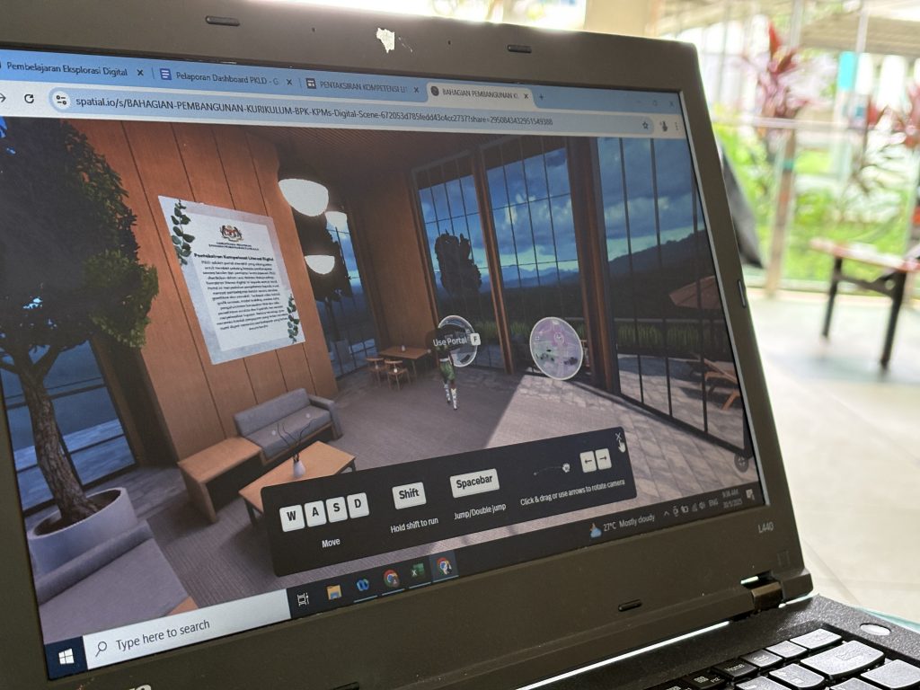
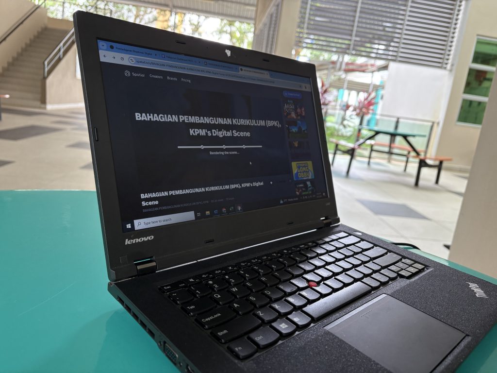
Met JPN officer to discuss on the Metaverse and its potential in pedagogy. Looking forward to this collab as I believe it has a good potential moving forward.

Recording session for MC courses for the subject BTE1522 – Raspberry Pi.
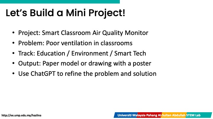
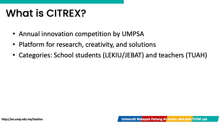
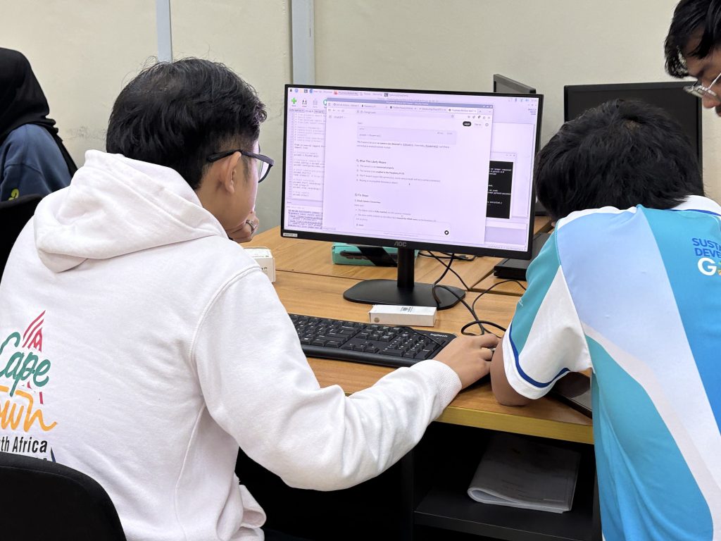
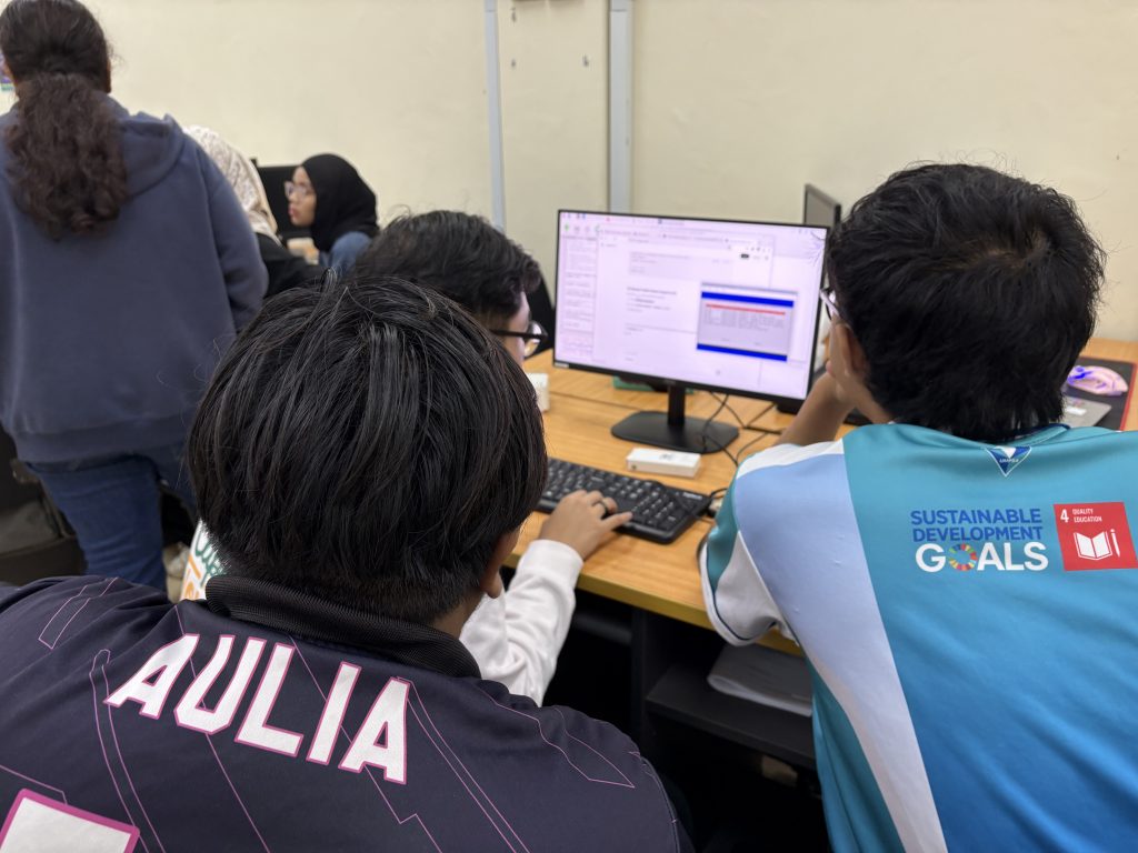
Today, we had the opportunity to host a hands-on innovation workshop for students from 21 schools in the Pekan District, in collaboration with Pejabat Pendidikan Daerah Pekan. The workshop, held at UMPSA STEM Lab, aimed to equip students with the tools and thinking frameworks needed to kickstart their journey toward the CITREX Innovation Competition 2025.
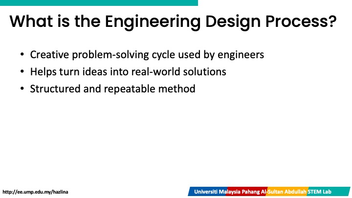
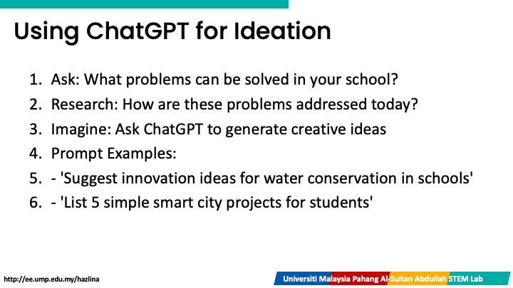
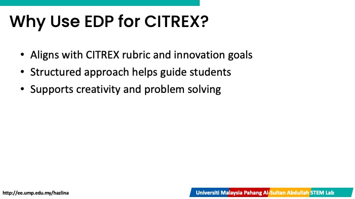
At the heart of this session was the Engineering Design Process (EDP)—a proven method used by engineers and innovators to solve real-world problems. But we added a modern twist – Generative AI, the new study buddy ChatGPT =).
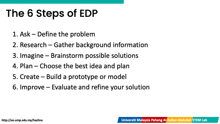
The Engineering Design Process (EDP)
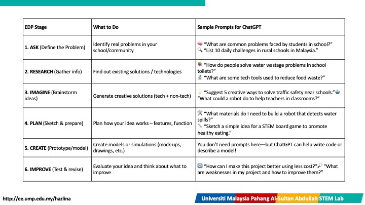
Students were guided through the six stages of EDP:-
Ask – Define a real problem
Research – Explore what’s already out there
Imagine – Brainstorm multiple ideas
Plan – Choose the best idea and sketch a solution
Create – Build a model or mock-up
Improve – Evaluate and enhance the design
Using the EDP worksheet, students documented their thinking and structured their innovation journey.
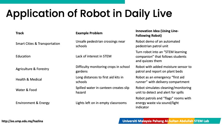
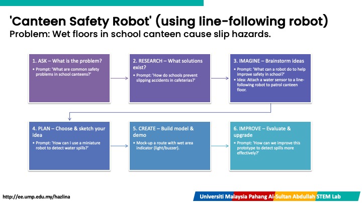
Many students in the session were already familiar with line-following miniature robots. We explored how these robots could be repurposed to solve problems aligned with CITREX themes such as:
Smart Cities – A robot that patrols school zones for safety
Environment – A robot that detects energy waste in classrooms
Health – A robot that simulates delivery of emergency medical supplies
By rethinking what they already had, students realized how innovation is often about new context, not just new tech.
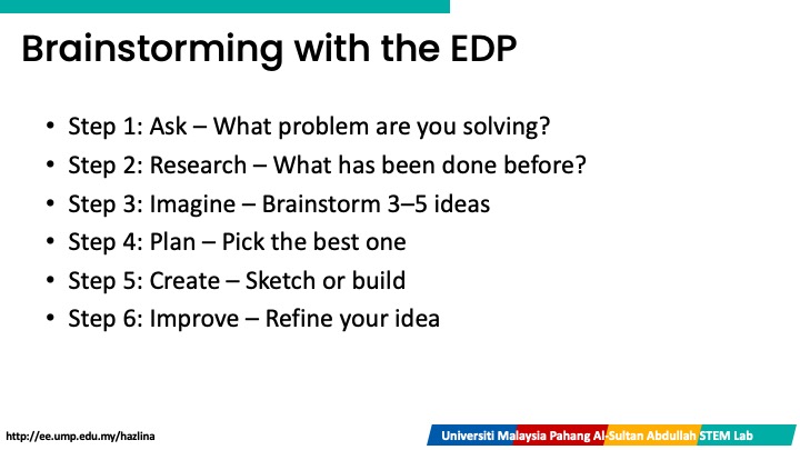
Students were introduced to the power of prompting ChatGPT effectively to support their ideation. We explored how to:
Ask the right questions
Frame problems clearly
Use follow-up prompts to refine and improve ideas
For example:
“What problems can a line-following robot solve in a school environment related to water safety?”
Students then tried these prompts themselves and saw how AI could boost the ‘Ask’ and ‘Research’ stages of the EDP.
Hands-On Practice
With their EDP worksheets in hand, students crafted project ideas guided by both human creativity and AI support. They were encouraged to:
Explore one of the nine CITREX themes
Develop an innovation using or modifying existing classroom tools
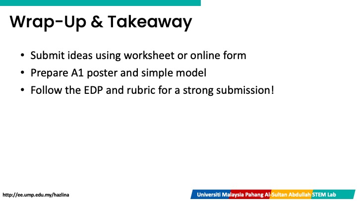
Prepare for submission with A1 posters and working models
This session was just the beginning. As we move toward CITREX 2025, we hope to see these young innovators continue developing their ideas into real solutions that can make a difference—in schools, communities, and beyond.
We thank all the participating schools and Pejabat Pendidikan Daerah Pekan for their commitment to fostering creativity and innovation among students.
Stay tuned for more workshops and updates from UMPSA STEM Lab =) !


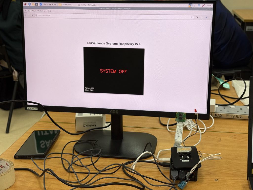
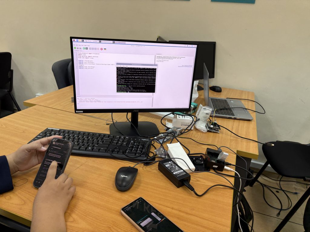
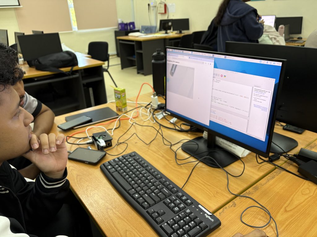
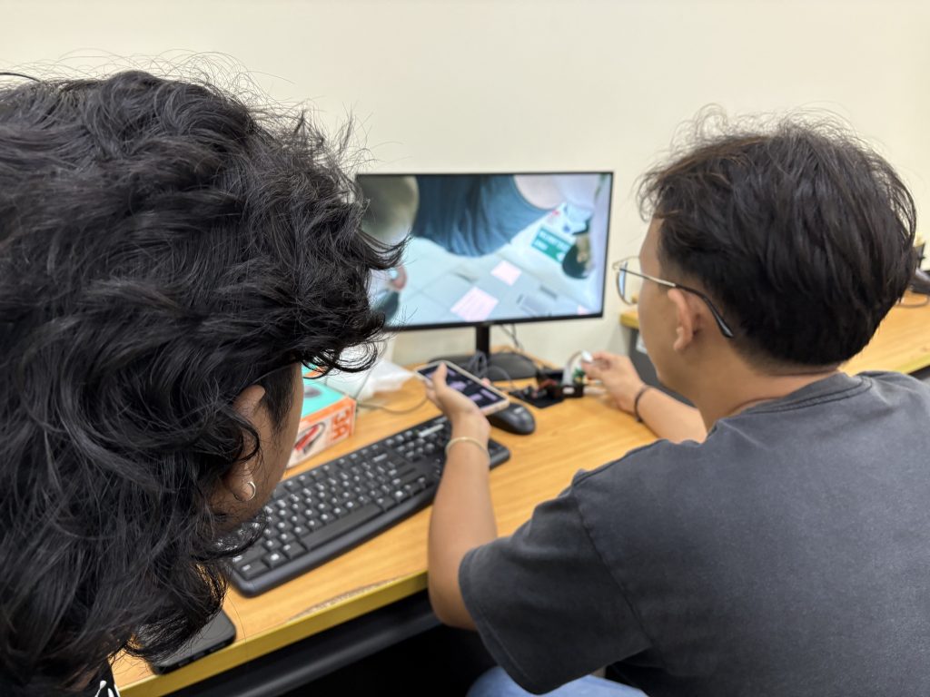
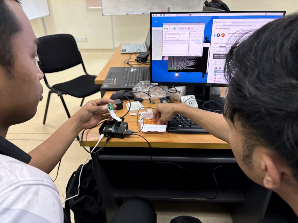
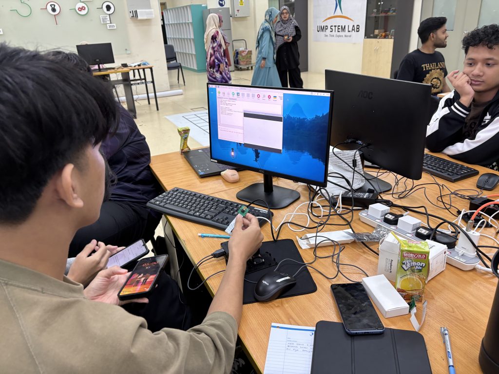
Today’s class in BTE1522 was packed with hands-on activities that introduced students to real-world applications of Raspberry Pi 4, focusing on camera integration and project development. The session was divided into two key sections, each playing an important role in reinforcing both technical knowledge and project-based learning.
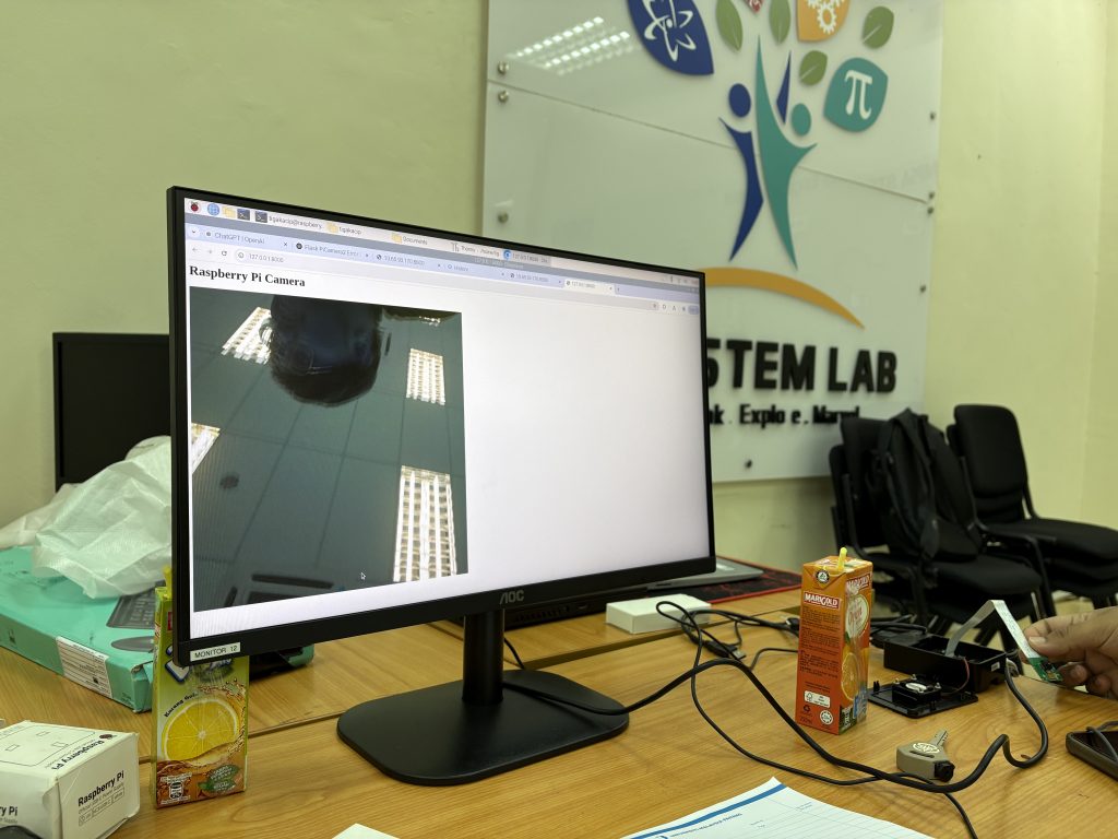
Section 1: Raspberry Pi Camera Module – From Capture to Streaming
The first half of the class focused on working with the Raspberry Pi camera module, a fundamental tool in the world of image processing and artificial intelligence. Students learned:
How to capture still images using Python and Raspberry Pi’s built-in libraries.
How to initiate video streaming using the PiCamera and OpenCV, preparing them for real-time image processing applications.


These activities are not just about capturing visuals—they serve as a gateway to advanced applications like image classification, object detection, and AI-based recognition systems.
This reminded me to a project from a previous semester, where one of our students successfully developed an image detection system using the same setup. The project was able to identify a variety of items like books, pencils, and even human figures—an impressive feat for a class-based project!
Today’s session laid the groundwork for such possibilities, and we’re excited to see how current students might push the boundaries even further.
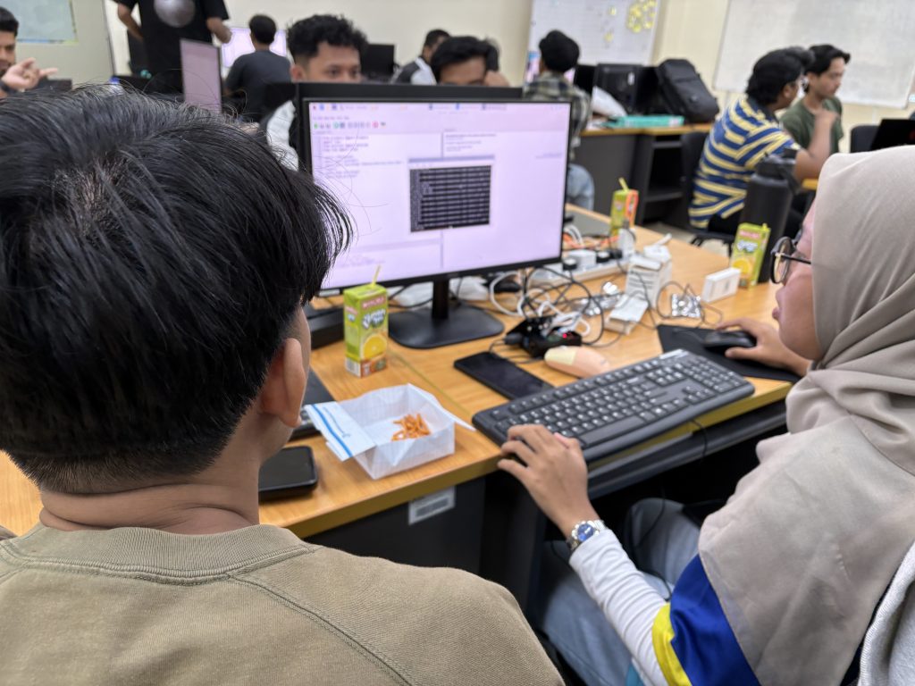
Section 2: Project Development Begins
The second part of the session shifted focus toward the students’ individual and group projects. This semester, we’ve offered 9 project titles, each designed to challenge students to apply what they’ve learned across programming, electronics, and embedded systems.
During this session, students –
Began structuring their project workflow.
Identified the core components and sensors required.
Discussed functional requirements and potential integration challenges.
Started early-stage coding and circuit prototyping.
This segment highlighted the importance of hands-on learning, collaborative teamwork, and practical application of theory.
Today’s class was not just about technical instruction—it was about igniting curiosity and innovation. Whether it’s capturing a simple image or streaming live video, each activity builds toward something bigger. Combined with project-based learning, students are not just coding—they’re creating, solving problems, and applying technology in meaningful ways.
Looking forward to seeing how each of the nine projects evolve over the coming weeks. As always, proud of the effort and enthusiasm shown by everyone in class today.


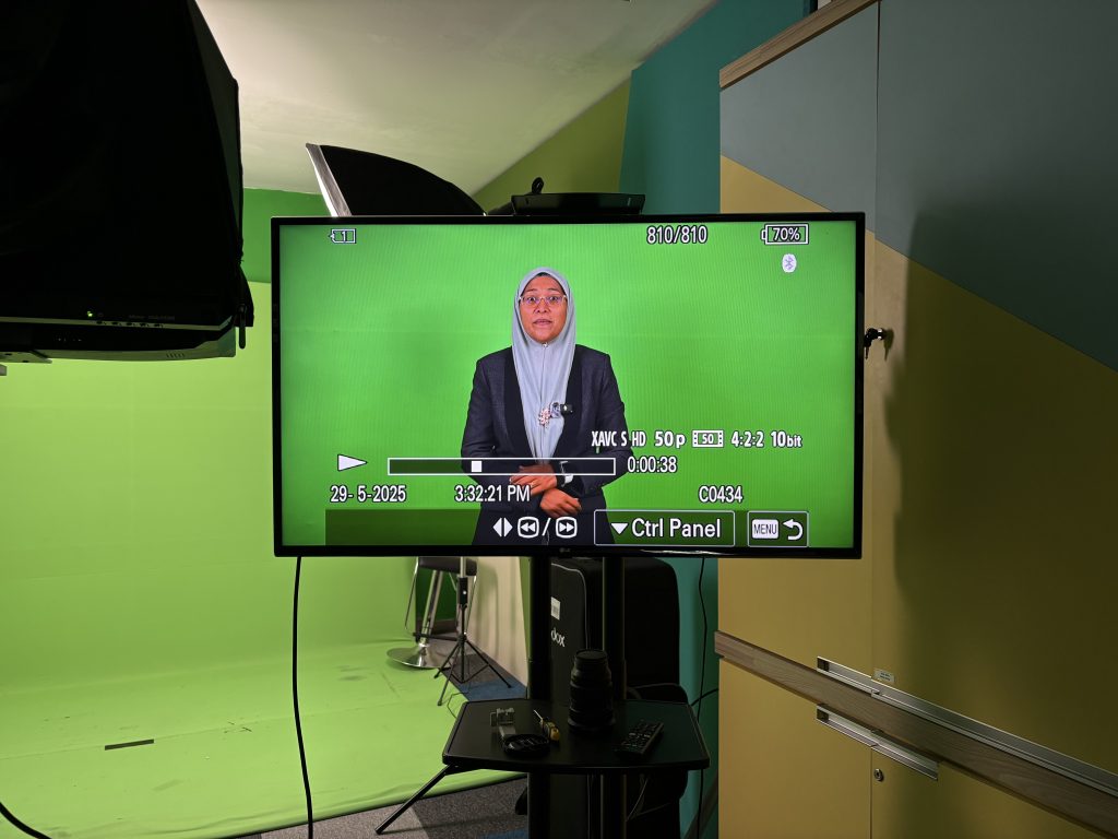
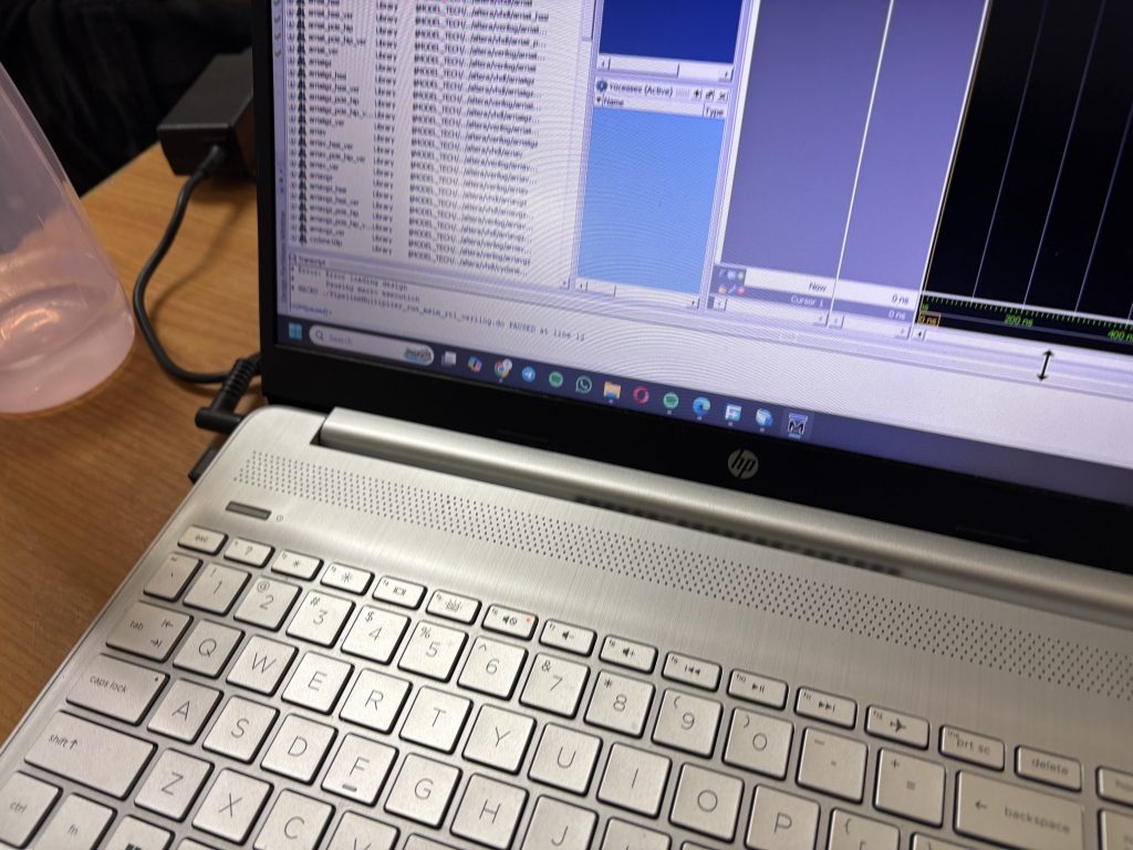
Today we look into one of the most critical yet often overlooked topics in FPGA design – Static Timing Analysis (STA). Understanding STA is key to ensuring that your digital design works not only functionally but also reliably at speed. To ground this theoretical topic, students also completed Lab 5, where they compared pipelined and non-pipelined multipliers and analyzed timing and performance parameters.
What Is Static Timing Analysis?
Static Timing Analysis is a method used to determine if a digital circuit will operate correctly at the target clock frequency without needing simulation input vectors. It uses timing constraints and logic paths to compute:
Setup time
Hold time
Propagation delay
Rise and fall times
Clock skew
Critical path delay
Maximum clock frequency
The goal is to verify that all data signals arrive where they need to, on time, under worst-case conditions.
Key Timing Parameters Explained
To help visualize the concept, we used a simple design involving two D Flip-Flops (FF1 and FF2) connected through a combinational logic block composed of two logic gates.
1. Setup Time
This is the minimum time the data must be stable before the clock edge arrives at FF2. If violated, data may not be correctly latched.
2. Hold Time
The data must remain stable after the clock edge. If violated, metastability may occur.
3. Propagation Delay
This is the time taken for the signal to travel through the logic gates between FF1 and FF2. It’s dependent on the type and number of gates.
4. Rising/Falling Time
The transition period from low to high or high to low in the signal waveform. Faster transitions are better for minimizing timing uncertainty.
5. Clock Skew
This occurs when the clock arrives at FF1 and FF2 at slightly different times. Clock skew can reduce the effective timing margin.
Example in Class Two Flip-Flops and Logic Path
Imagine a logic path between FF1 (source) and FF2 (destination)
Let’s assume-

Propagation delay through AND = 2ns
Propagation delay through OR = 3ns
Setup time of FF2 = 1ns
Clock skew = 0.5ns
Then, the total delay from FF1 to FF2 is –
To meet setup time, the clock period must be at least:
This gives a maximum clock frequency of:
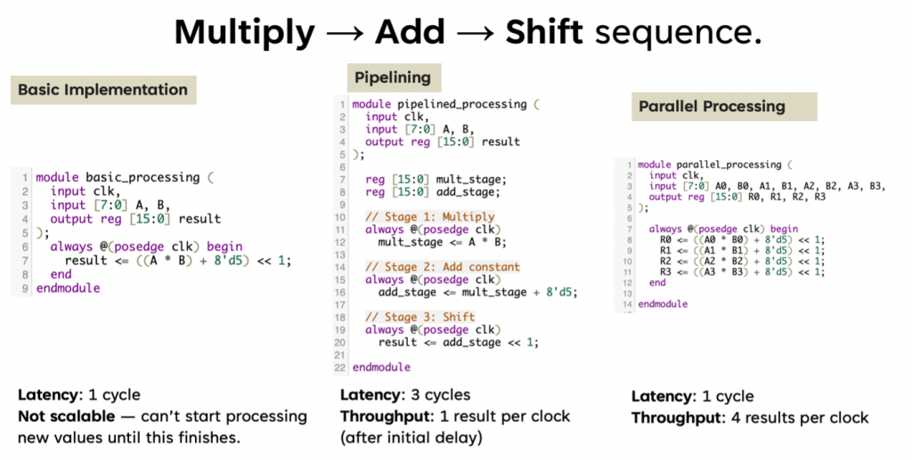
In Lab 5, students implemented and tested two versions of a multiplier:
Non-Pipelined Multiplier – Straightforward, all computation happens in one clock cycle.
Pipelined Multiplier – Operation split into multiple stages with registers (flip-flops) in between.
They then analyzed the following performance metrics – (hypothetically =))
| Parameter | Non-Pipelined | Pipelined |
|---|---|---|
| Critical Path Delay | Higher | Lower |
| Max Clock Frequency | Lower | Higher |
| FPGA Logic Utilization | Lower | Higher |
| Throughput | Lower | Higher (1 output per cycle after latency) |
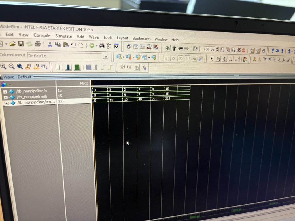
Pipelining reduces the critical path delay, allowing the design to run at a much higher clock frequency.
While pipelining increases the logic utilization (more flip-flops), the throughput improves significantly, making it ideal for high-speed applications like real-time data processing in picosatellites or image processing.
Static timing analysis helps quantify the improvements, giving insight into real performance beyond just functional correctness.
See you next week for your FPGA project development =)
Job well done everyone!
In this assignment, students of BTE1522 are required to modify the Slider Game with the following requirements:-

