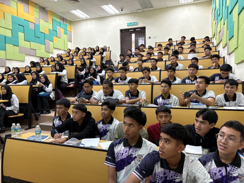
BTE1522 – Week 13 – Project Development

Over the past three weeks, our BTE1522 class transitioned into full project-based learning mode, where students were tasked to apply all they have learned throughout the semester—from Python programming basics to hardware interfacing with the Raspberry Pi 4. This phase was not just about completing an assignment—it was about creating functional, working solutions from scratch.

Each group (consisting of three students) was equipped with:

      1. A UMPSA STEM Cube

      2. Raspberry Pi 4

      3. Camera Module

      4. GPS Sensor

      5. BME280 (temperature, humidity, pressure)

      6. MPU6050 (accelerometer and gyroscope)

Students selected one topic from a set of project assignments, all of which required multidisciplinary skills. Each project had to include the following components:

      1. Sensor Integration: Establish working connections between Raspberry Pi and the sensors.

      2. Data Storage: Build a working database—either local (e.g., SQLite) or cloud-based (e.g., Firebase, Google Sheets).

      3. Dashboard Development: Create a working user interface/dashboard using tools like Streamlit, Flask, Adafruit IO, or Blynk to visualize data and system status.

The Learning Process

This phase was entirely project-based, meaning students were expected to learn through experimentation, debugging, and problem-solving. Unlike guided tutorials, this process encouraged independent learning and collaboration:

      1. Debugging wiring errors

      2. Fixing Python runtime bugs

      3. Reading sensor data accurately

      4. Sending and retrieving data from a database

      5. Building interactive visual dashboards

Learning programming—especially physical computing—is most effective when you’re actually doing it. The moment something doesn’t work, and you have to troubleshoot, is when you truly begin to understand what you’re building. the most important thing is NOT TO GIVE UP 🙂

This project based learning phase is aimed at solidifying  concepts from earlier weeks, including:

      1. Python functions and loops

      2. Conditional logic

      3. File and data handling

      4. Sensor reading and real-time feedback

      5. REST APIs and interface design

Final Submission Checklist

As the project phase concludes, students are required to submit their work via KALAM. Each group should prepare:

      1. A complete lab report

      2. A 3-minute walkthrough video, demonstrating the system and explaining their code

      3. A zip folder with all Python source code files

This final submission will serve not only as a record of their accomplishment but also as a mini portfolio piece showcasing their ability to develop real-world solutions.

Each team faced unique challenges, but everyone succeeded in developing a working prototype with analytics. This hands-on, integrative experience truly brings the course’s learning outcomes to life.

Looking forward to your final presentations and submission in KALAM next week. Great job, everyone—keep building and keep learning!


FYP/SDP Progress Meeting and Discussion with JPN

FYP/SDP Progress

Very well done, everyone is progressing well with the targeted milestones. Out framework consists of sensor integration, database and dashboard.

Everyone is on track – ready to infuse intelligence /image processing to the system.

Discussion JPN Pahang

Met JPN officer to discuss on the Metaverse and its potential in pedagogy. Looking forward to this collab as I believe it has a good potential moving forward.

Enngineering Design Process and Robot Innovation and Application (Citrex 2025 Workshop)

Today, we had the opportunity to host a hands-on innovation workshop for students from 21 schools in the Pekan District, in collaboration with Pejabat Pendidikan Daerah Pekan. The workshop, held at UMPSA STEM Lab, aimed to equip students with the tools and thinking frameworks needed to kickstart their journey toward the CITREX Innovation Competition 2025.

At the heart of this session was the Engineering Design Process (EDP)—a proven method used by engineers and innovators to solve real-world problems. But we added a modern twist – Generative AI, the new study buddy ChatGPT =).

The Engineering Design Process (EDP)

Students were guided through the six stages of EDP:-

  1. Ask – Define a real problem

  2. Research – Explore what’s already out there

  3. Imagine – Brainstorm multiple ideas

  4. Plan – Choose the best idea and sketch a solution

  5. Create – Build a model or mock-up

  6. Improve – Evaluate and enhance the design

Using the EDP worksheet, students documented their thinking and structured their innovation journey.

Many students in the session were already familiar with line-following miniature robots. We explored how these robots could be repurposed to solve problems aligned with CITREX themes such as:

  1. Smart Cities – A robot that patrols school zones for safety

  2. Environment – A robot that detects energy waste in classrooms

  3. Health – A robot that simulates delivery of emergency medical supplies

By rethinking what they already had, students realized how innovation is often about new context, not just new tech.

Students were introduced to the power of prompting ChatGPT effectively to support their ideation. We explored how to:

  1. Ask the right questions

  2. Frame problems clearly

  3. Use follow-up prompts to refine and improve ideas

For example:

“What problems can a line-following robot solve in a school environment related to water safety?”

Students then tried these prompts themselves and saw how AI could boost the ‘Ask’ and ‘Research’ stages of the EDP.

Hands-On Practice

With their EDP worksheets in hand, students crafted project ideas guided by both human creativity and AI support. They were encouraged to:

  1. Explore one of the nine CITREX themes

  2. Develop an innovation using or modifying existing classroom tools

  3. Prepare for submission with A1 posters and working models

Looking Ahead

This session was just the beginning. As we move toward CITREX 2025, we hope to see these young innovators continue developing their ideas into real solutions that can make a difference—in schools, communities, and beyond.

We thank all the participating schools and Pejabat Pendidikan Daerah Pekan for their commitment to fostering creativity and innovation among students.

Stay tuned for more workshops and updates from UMPSA STEM Lab =) !


BTE1522 – Innovation – Week 10 – Camera Module

Today’s class in BTE1522 was packed with hands-on activities that introduced students to real-world applications of Raspberry Pi 4, focusing on camera integration and project development. The session was divided into two key sections, each playing an important role in reinforcing both technical knowledge and project-based learning.

Section 1: Raspberry Pi Camera Module – From Capture to Streaming

The first half of the class focused on working with the Raspberry Pi camera module, a fundamental tool in the world of image processing and artificial intelligence. Students learned:

  1. How to capture still images using Python and Raspberry Pi’s built-in libraries.

  2. How to initiate video streaming using the PiCamera and OpenCV, preparing them for real-time image processing applications.

These activities are not just about capturing visuals—they serve as a gateway to advanced applications like image classification, object detection, and AI-based recognition systems.

This reminded me to a project from a previous semester, where one of our students successfully developed an image detection system using the same setup. The project was able to identify a variety of items like books, pencils, and even human figures—an impressive feat for a class-based project!

Today’s session laid the groundwork for such possibilities, and we’re excited to see how current students might push the boundaries even further.

Section 2: Project Development Begins

The second part of the session shifted focus toward the students’ individual and group projects. This semester, we’ve offered 9 project titles, each designed to challenge students to apply what they’ve learned across programming, electronics, and embedded systems.

During this session, students –

  • Began structuring their project workflow.

  • Identified the core components and sensors required.

  • Discussed functional requirements and potential integration challenges.

  • Started early-stage coding and circuit prototyping.

This segment highlighted the importance of hands-on learning, collaborative teamwork, and practical application of theory.

Today’s class was not just about technical instruction—it was about igniting curiosity and innovation. Whether it’s capturing a simple image or streaming live video, each activity builds toward something bigger. Combined with project-based learning, students are not just coding—they’re creating, solving problems, and applying technology in meaningful ways.

Looking forward to seeing how each of the nine projects evolve over the coming weeks. As always, proud of the effort and enthusiasm shown by everyone in class today.


BHE3233 – Week 10 – Static Timing Analysis


Today we look into one of the most critical yet often overlooked topics in FPGA design – Static Timing Analysis (STA). Understanding STA is key to ensuring that your digital design works not only functionally but also reliably at speed. To ground this theoretical topic, students also completed Lab 5, where they compared pipelined and non-pipelined multipliers and analyzed timing and performance parameters.

What Is Static Timing Analysis?

Static Timing Analysis is a method used to determine if a digital circuit will operate correctly at the target clock frequency without needing simulation input vectors. It uses timing constraints and logic paths to compute:

  • Setup time

  • Hold time

  • Propagation delay

  • Rise and fall times

  • Clock skew

  • Critical path delay

  • Maximum clock frequency

The goal is to verify that all data signals arrive where they need to, on time, under worst-case conditions.

Key Timing Parameters Explained

To help visualize the concept, we used a simple design involving two D Flip-Flops (FF1 and FF2) connected through a combinational logic block composed of two logic gates.

1. Setup Time

This is the minimum time the data must be stable before the clock edge arrives at FF2. If violated, data may not be correctly latched.

2. Hold Time

The data must remain stable after the clock edge. If violated, metastability may occur.

3. Propagation Delay

This is the time taken for the signal to travel through the logic gates between FF1 and FF2. It’s dependent on the type and number of gates.

4. Rising/Falling Time

The transition period from low to high or high to low in the signal waveform. Faster transitions are better for minimizing timing uncertainty.

5. Clock Skew

This occurs when the clock arrives at FF1 and FF2 at slightly different times. Clock skew can reduce the effective timing margin.

Example in Class Two Flip-Flops and Logic Path

Imagine a logic path between FF1 (source) and FF2 (destination)

FF1 ----> [AND Gate] ---> [OR Gate] ---> FF2

Let’s assume-

  • Propagation delay through AND = 2ns

  • Propagation delay through OR = 3ns

  • Setup time of FF2 = 1ns

  • Clock skew = 0.5ns

Then, the total delay from FF1 to FF2 is –

2ns (AND) + 3ns (OR) = 5ns

To meet setup time, the clock period must be at least:

arduino
Total delay + Setup time + Skew = 5ns + 1ns + 0.5ns = 6.5ns

This gives a maximum clock frequency of:

1 / 6.5ns ≈ 153.8 MHz

Lab 5 – Pipelining vs Non-Pipelining in Multiplier Design

In Lab 5, students implemented and tested two versions of a multiplier:

  • Non-Pipelined Multiplier – Straightforward, all computation happens in one clock cycle.

  • Pipelined Multiplier – Operation split into multiple stages with registers (flip-flops) in between.

They then analyzed the following performance metrics – (hypothetically =))

Parameter Non-Pipelined Pipelined
Critical Path Delay Higher Lower
Max Clock Frequency Lower Higher
FPGA Logic Utilization Lower Higher
Throughput Lower Higher (1 output per cycle after latency)
  • Pipelining reduces the critical path delay, allowing the design to run at a much higher clock frequency.

  • While pipelining increases the logic utilization (more flip-flops), the throughput improves significantly, making it ideal for high-speed applications like real-time data processing in picosatellites or image processing.

  • Static timing analysis helps quantify the improvements, giving insight into real performance beyond just functional correctness.

See you next week for your FPGA project development =)

BHE3233 – Week 9 – Finite State Machine

Today’s class focused on one of the core topics in digital system design—Finite State Machines (FSM)—through an engaging and practical activity: building a 101 sequence detector using a Moore machine.

We began with a recap of FSM fundamentals—specifically the Moore machine, where outputs are solely determined by the current state. This conceptual understanding paved the way for the day’s main activity: designing and testing a sequence detector that identifies the binary pattern 101.

Key areas explored:

  1. State transition diagrams and state encoding

  2. Implementation using case statements

  3. Exploring both dataflow-style FSM and conditional (if-else) statement-based FSMs

  4. Synthesizing and testing using Quartus Prime

Students designed the FSM in Verilog using Quartus. The Moore machine was structured with three states to detect the pattern:

  1. S0 – Initial state

  2. S1 – Received ‘1’

  3. S2 – Received ‘10’

When the full sequence 101 was detected, the FSM output went high.

always @(posedge clk or posedge reset) begin
if (reset)
state <= S0;
else begin
case(state)
S0: state <= (in == 1) ? S1 : S0;
S1: state <= (in == 0) ? S2 : S1;
S2: state <= (in == 1) ? S1 : S0;
endcase
end
end

Simulation and Testbench Creation

To validate the design, students created testbenches that simulated input sequences. Using ModelSim, they:

  • Applied a sequence of 0s and 1s to the in input

  • Monitored state transitions

  • Verified output pulses when 101 was detected

This phase helped students understand the role of simulation in design verification and how FSMs react to clocked inputs in real time.

The case statement simplified FSM implementation, especially when compared to nested conditional (if-else) logic. They also discussed how a well-structured FSM can lead to clean, readable, and maintainable RTL code—an essential practice in real-world design.

Learning Outcomes

By the end of the session, students were able to:

  1. Describe and implement Moore FSMs in Verilog

  2. Translate a sequence detection problem into state transitions

  3. Use Quartus for synthesis and ModelSim for simulation

  4. Compare dataflow FSM vs. conditional FSM modeling