


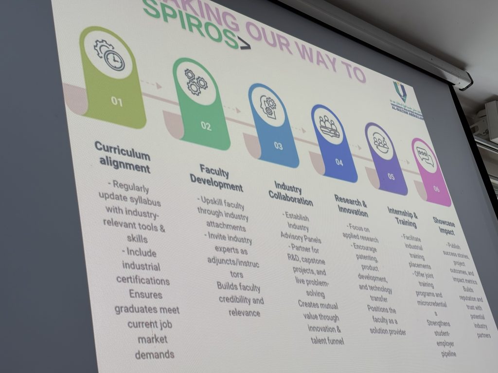
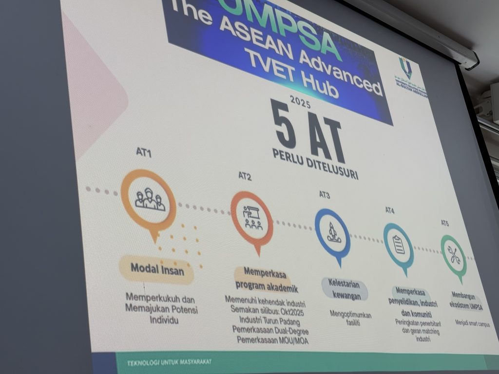
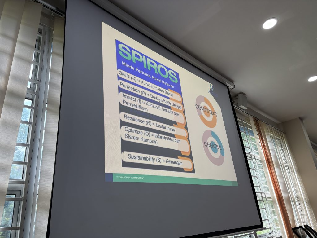
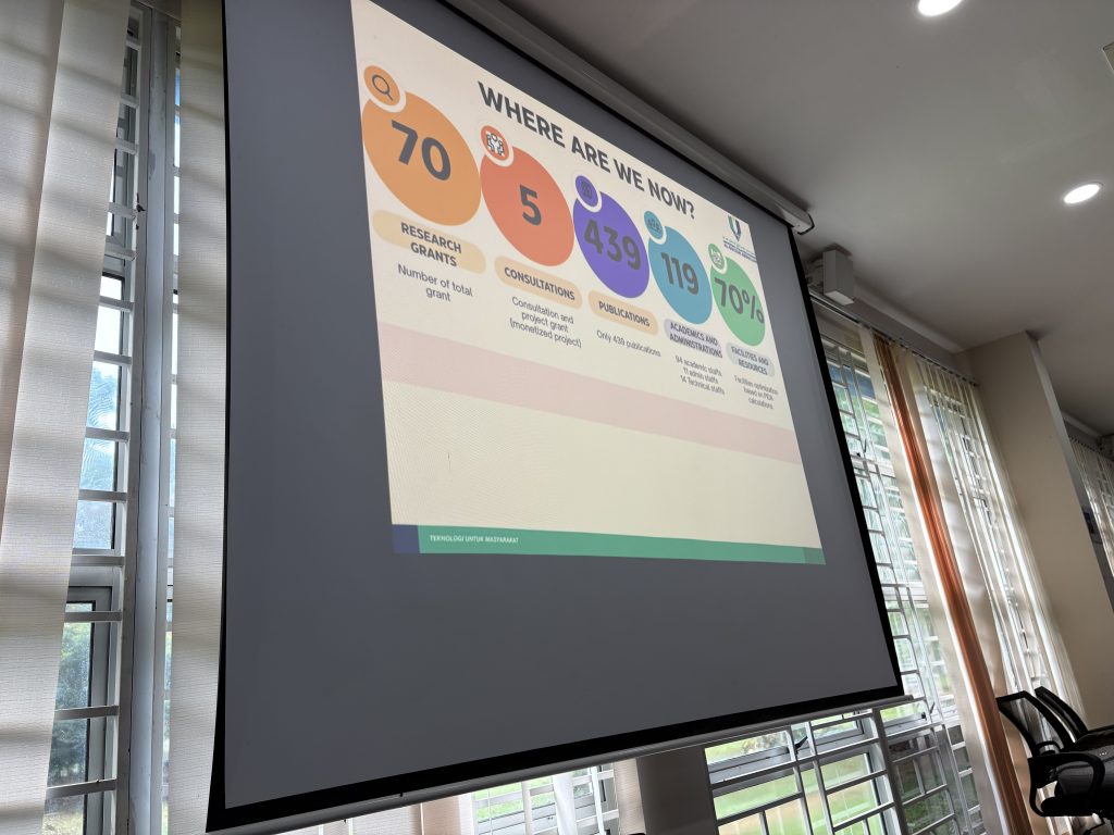
The world is digital, but life is analog..


Well done =)


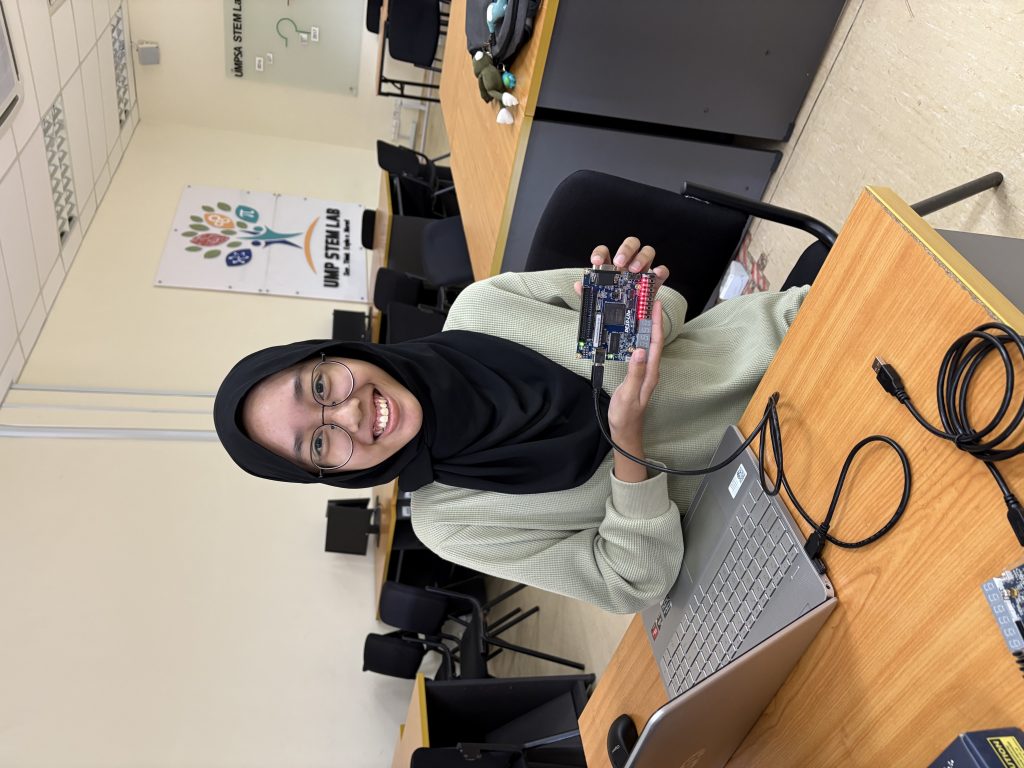
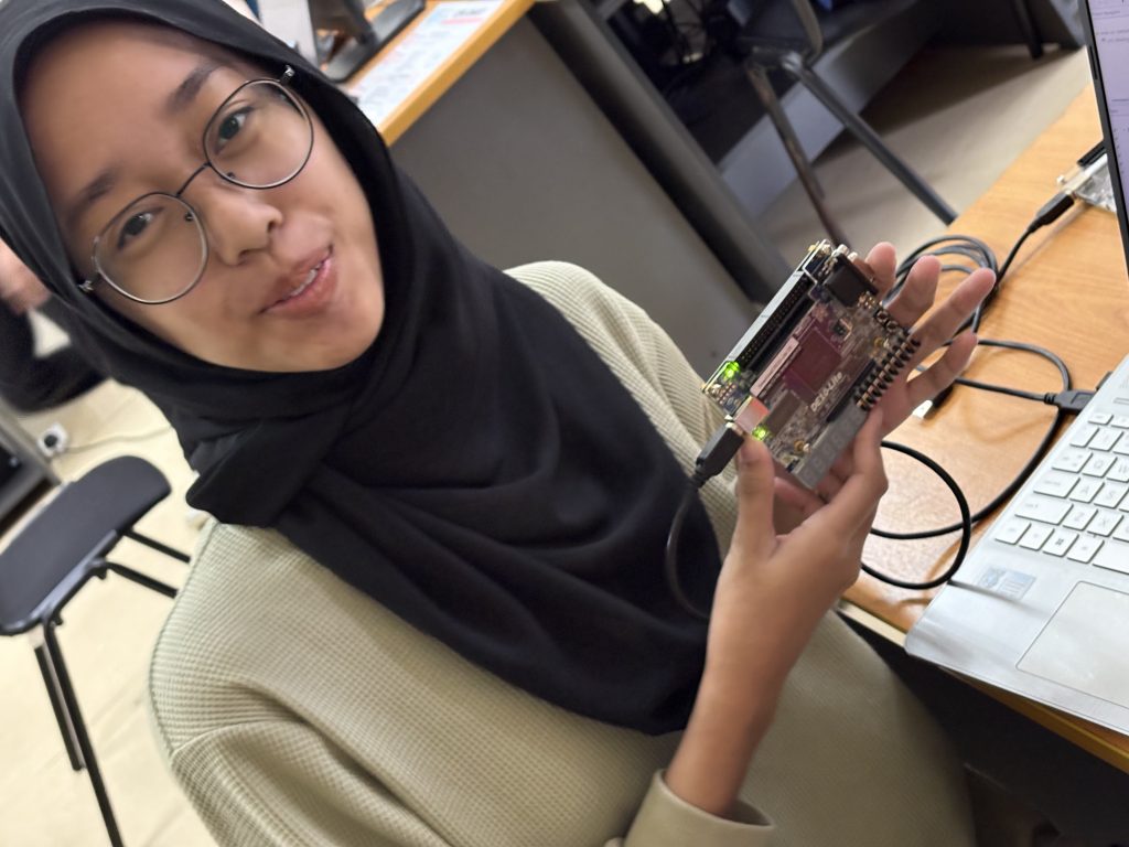
This week, students in the BHE3233: Hardware Description Language course took on three lab activities using the Altera DE10-Lite FPGA board. These labs were designed to deepen their understanding of digital logic design, from real hardware control to simulation-level debugging using testbenches.
Lab 1 Recap: LED Blinking with Verilog
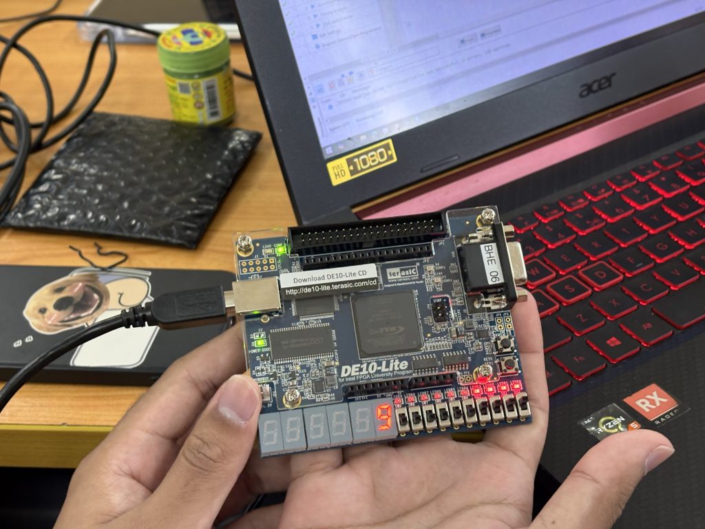
Students developed a Verilog module to blink the 10 onboard LEDs one at a time in sequence, based on a timing counter. The project introduced:
always @(posedge clk)
Counter logic for delay generation
reg and assign statements for driving output
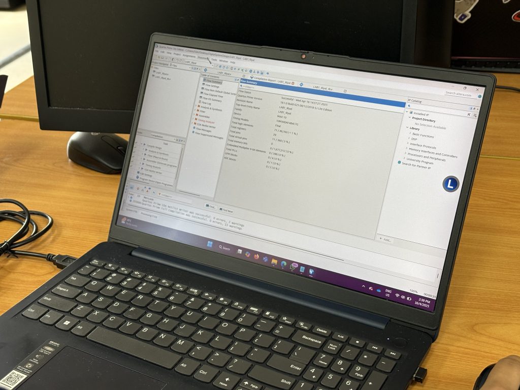
Pin assignment in Quartus
Lab 2 Recap: Real-Time LED Control Using Slider Switches
Students mapped the 10 slider switches directly to the 10 LEDs using basic combinational logic. This hands-on activity helped reinforce:
Use of continuous assignment (assign)
Bit-wise mapping between inputs and outputs
How to apply pin mapping in Quartus for SW[9:0] and LED[9:0]
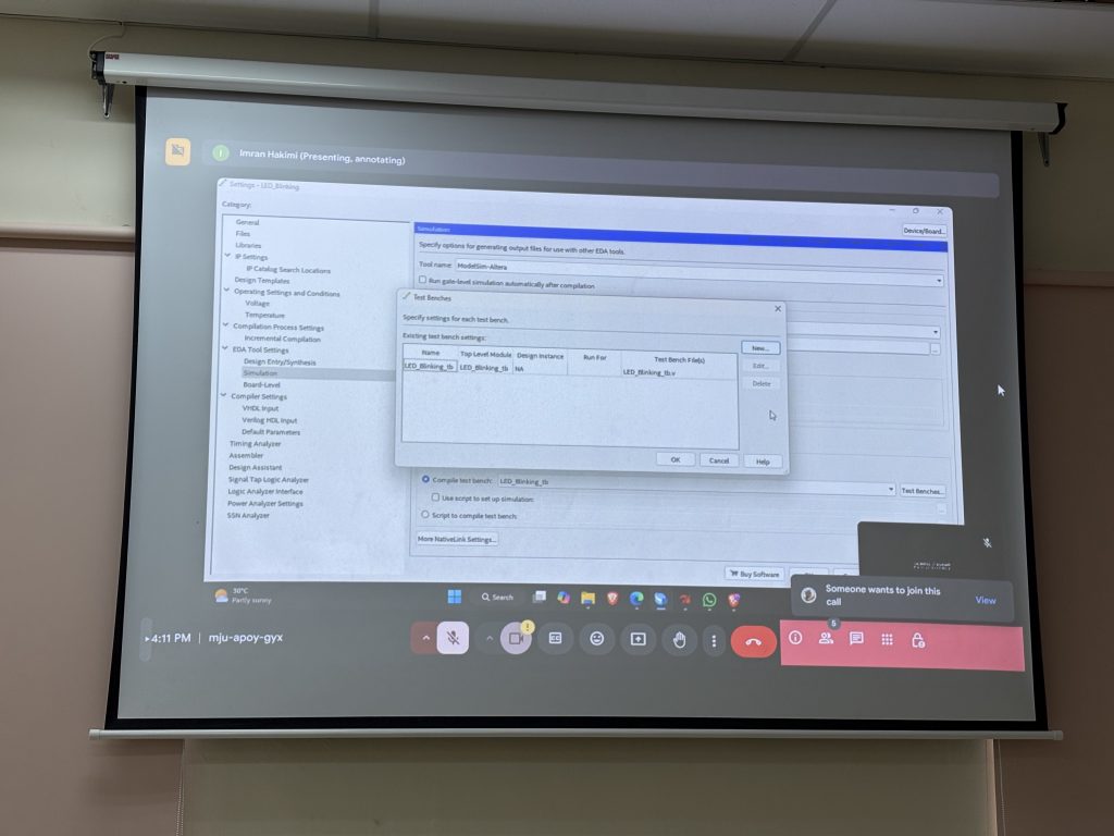
Lab 3 Preview: Writing a Testbench & Understanding Timing Diagrams
To develop a testbench for both Lab 1 (LED Blinking) and Lab 2 (Switch to LED) designs, simulate the behavior using ModelSim, and interpret the timing diagram (waveform) to verify correct functionality.
ModelSim (Intel FPGA Edition) for running simulations
Waveform viewer for analyzing signal transitions over time
To Do
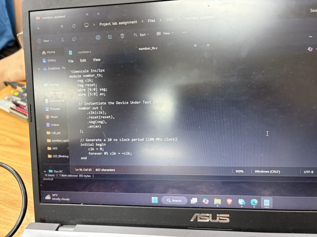
Create a Testbench File for Each Design
Instantiate the DUT (Design Under Test)
Simulate clk signal (for Lab 1)
Apply appropriate test vectors (SW[9:0]) for Lab 2
Run Simulation
Launch ModelSim from Quartus
Compile and simulate the testbench
Observe and save waveform output
Analyze the Timing Diagram
For Lab 1: Check the blinking behavior of LED[current_led]
For Lab 2: Confirm that LED outputs match the SW inputs at each simulation step
Learning Outcome:
Students will visually interpret digital signal transitions through the waveform viewer in ModelSim, reinforcing:
Propagation delay
Clock edge behavior
Signal assertion and response timing
Apply Hardware Description Languages (HDL) to design, simulate, and verify digital circuits at the Register Transfer Level (RTL).
Lab 3 bridges the gap between coding and functional verification. Students now understand how simulation helps confirm logic correctness before moving to hardware.
What’s Next?
Next week, you will begin working on combinational building blocks like adders and multipliers, then explore state machines and RTL synthesis in depth.
and Midterm Test 🙂